By DOUGLAS SELF
Douglas Self describes the problems of designing MC head amplifiers and illustrates them by means of a new design, originally intended for use with his precision preamplifier.
In recent years, moving-coil cartridges have increased greatly in popularity. This is not the place to try and determine if their extra cost is justified by an audible improved performance; suffice it to say that a preamplifier now needs a capable moving-coil cartridge input if it is to be considered complete. The head-amplifier design presented here as an example was originally intended to be retrofitted to the precision preamplifier previously published in Wire less World', feeding the existing moving-magnet disc input. However it is adaptable to almost any preamplifier and cartridge as the gain range available is very wide; it should therefore be of interest to any engineer working in this field. Hereafter "moving coil" is abbreviated to MC, and "moving-magnet" to MM.
Traditionally, moving-coil cartridges were matched to moving-magnet inputs by special transformers, which give "free gain"--in a sense--and are capable of a good noise performance if the windings are carefully designed for very low series resistance.
However, the inescapable problems of low-frequency distortion, high-frequency transient overshoots and the need for obsessive screening to avoid 50Hz mains pickup render them unattractive and expensive.
The requirements for a high-quality MC head-amplifier are as follows. The over whelming need is for a good noise performance, as the signals generated by MC cartridges are, in general, very low. However, this sensitivity is also much more vari able than that of MM cartridges, where one can take a nominal output of 5mVr.m.s. for 5cm/s at 1kHz as being virtually standard. In contrast, a survey of the available MC cartridges gave a range from 2.35mV (Dynavector DV10X N) to 0.03mV (Audionote 102vdH), though these are both exceptional and the great majority fell between 0.2mV and 0.4mV. Figure 1 shows the output levels of a number of current MC cartridges plotted on a scale of dBu (i.e. referred to 775mV) and MM cartridges are included on the right for comparison. It is notable how these bunch together in a range of less than 7dB, A representative MC cartridge used both as a basis for design, and for testing, is the Ortofon MC10 Super, which has an output of 0.3mV for 5cm/s, and an internal resistance of 3 ohms. There is general agreement that this is a good-sounding component.
As detailed above, there is a need for easily variable gain over a wide range. This can be quite adequately provided in switched steps, avoiding the problems of uncertain stereo balance on dual potentiometers. From the above output figures, a gain range of 6dB to 46dB appears necessary to cater for all possible cartridges. It would seem, at the low-gain end, that the amplifier is virtually redundant, and so a minimum gain of 20dB was chosen.
Moving-coil cartridges are very tolerant of the loading they see at an amplifier's input, as a result of their own very low internal impedance. For example, Ortofon, who might be reckoned to know a thing or two about MC cartridges, simply state that the recommended load for most of their wide range of cartridges is "greater than 10 ohms". Nonetheless, since experimenting with cartridge loading is a harmless enough pastime, provision for changing the input loading resistor over a wide range has been made in this design.
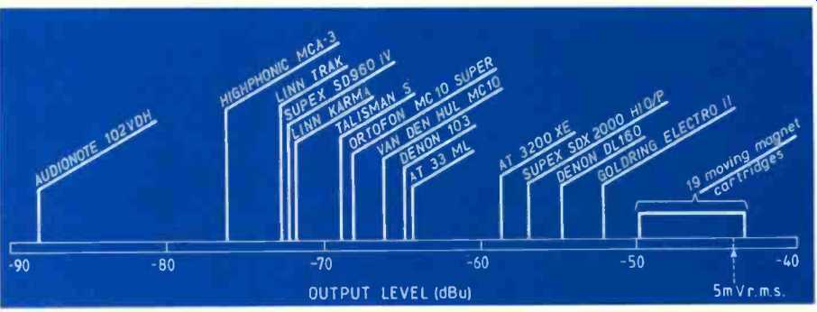
Fig. 1. Output levels of representative moving-coil cartridges plotted
on a scale of decibels relative to 0.775V (1mW in 600 ohms), with the outputs
of a number of moving-magnet cartridges as a comparison.
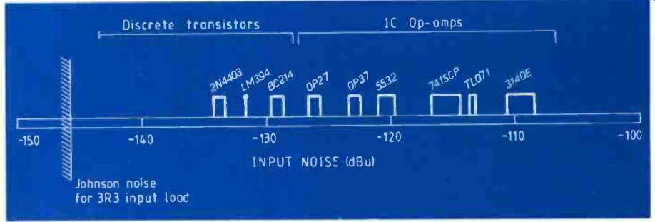
Fig. 2. Discrete transistors still, in the main, provide a better noise
performance than op-amps at low source resistances, as shown here for five
examples of each type.
The preamplifier should have the ability to drive a normal MM cartridge input at sufficient level to ensure that the head amplifier does not limit the disc headroom.
Any figure here over about 300mV r.m.s. should be satisfactory. A less obvious point is that the input impedance, apart from the nominal 47k resistive component, usually includes a fair amount of capacitance, either to adjust cartridge frequency response or to exclude r.f. This can cause head-amplifier instability unless it is dealt with.
Finally, a head amplifier should meet the usual requirements for frequency response, crosstalk, and linearity. Capacitive crosstalk is usually not a problem, due to the very low impedances involved, but for the same reason, linearity can present problems de spite the low signal levels.
DESIGN PROBLEMS
The theoretical noise characteristics of amplifiers have been dealt with very competently in other articles, and there is no need to repeat the various mathematical derivations here. The designer's options are usually limited to choosing a suitable input device, operating it at roughly the right current, (not usually critical due to the flat bottoms of the noise curves) and then making sure that the surrounding circuitry doesn't mess things up too much. MC head amplifiers are almost always built around discrete devices, with or without the addition of an accompanying op-amp (for an exception see Ref. 3.). Figure 2 shows the reason why: when source resistances are low (say below 1k) even advanced op-amps are easily out-performed by discrete devices, due to the inevitable compromises in IC fabrication. The values of equivalent input noise (e.i.n.) in Fig.2 were taken from five samples of each device, using a source resistance of 3R3, and the general circuit configuration in Fig.3. The rather non-standard measurement bandwidth is due to the use of the internal filters on a Sound Technology measuring system; adding a third-order 20 kHz active filter at the ST input would be very difficult, as the levels of noise being measured are so low. To convert to 20 kHz upper bandwidth limit, subtract 1.5dB. One of the prerequisites for good performance in this role is a low value for Rb, and this has led to a fine miscellany of devices being applied to a job they were never intended for: medium power devices, print-hammer drivers, (a lot of transistors seem to have been designed as print-hammer drivers) and so on.
Apart from careful device selection, the other classical way of reducing noise with low source impedances is to use multiple devices. The assumption here is that MC amplifier noise will swamp the miniscule Johnson noise inherent in the source (this is usually all too true) and therefore, if two input devices have their outputs summed, the signals will simply add, giving a 6dB gain, while the two uncorrelated device noise contributions will partially cancel, giving only 3dB.
Thus, there is a theoretical gain of 3dB in noise performance every time the number of input devices is doubled. There are, of course, clear economic limits to the amount of doubling you can go in for; eight parallel devices is the most that I have seen. It also seems difficult in practice to get the full theoretical benefit.
MC head-amplifiers in use today can be roughly divided into three common topologies, as shown in Fig. 4. That shown in 4(a) relies on a single device with low Rb, and the combination of limited open-loop gain and the heavy loading of the low-impedance of the feedback network on the final transistor means that both linearity and maximum output level tend to be uninspiring. Given the technical resources that electronics can deploy, there seems no need to ask the paying customers to put up with any measurable distortion at all. An amplifier of this type is analyzed in Ref. 4.
Figure 4(b) shows the classic multiple-parallel-transistor configuration; the amplifier block A is traditionally one or two discrete devices, that usually have difficulty in driving the low-impedance feedback net work. Effort is usually expended in ensuring proper current-sharing between the input devices.
This can be done by adding small emitter resistors to swamp VI, variations, but these will effectively appear in series with the source resistance, and compromise the noise performance unless they are individually decoupled with a row of very large electrolytics. Alternatively, each transistor can be given its own DC feedback loop to set up its collector current, but this tends to be even more prodigal of components. Having said this, experiment proved that the problem of current-sharing was not as serious as conventional wisdom holds; this is explained below. For examples of circuitry see Ref.5.
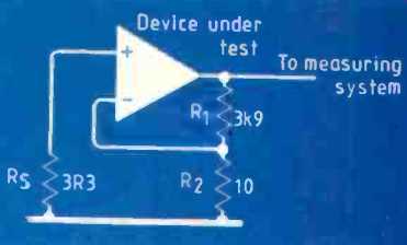
Fig. 3 Circuit used to obtain the measurements shown in Fig.2.
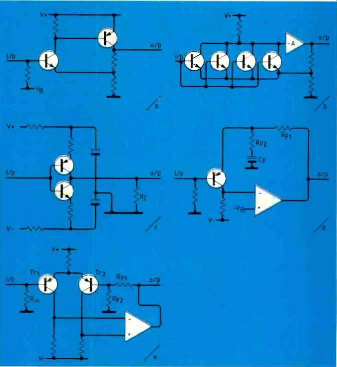
Fig. 4. Some head-amplifier configurations. A fairly low open-loop gain
in the circuit at (a) results in poor linearity. At (b), the gain is provided
by multiple transistors, which theoretically gives an improvement of 3dB
in noise performance for twice the number of transistors, but can also
present current-sharing problems. The arrangement at (c) provides the 3dB
improvement without current sharing: linearity is not of the highest order.
Circuit (d) uses one input device, the gain being provided by an op-amp:
the necessity for Cf presents problems, which are overcome in the (e) configuration
at the expense of a lowered noise performance.
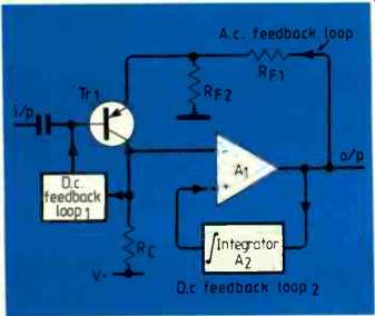
Fig. 5. The layout adopted for the final design.
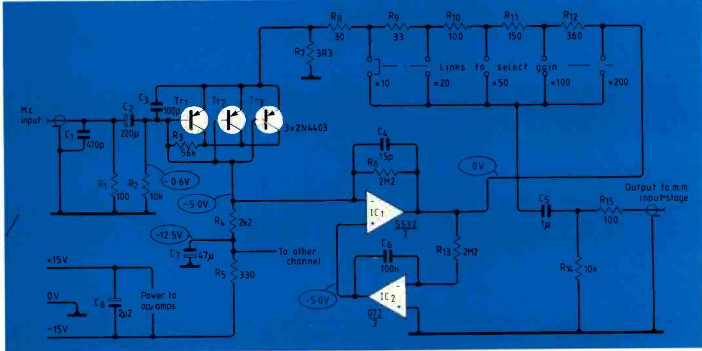
Fig. 6. Complete circuit diagram of the moving-coil head amplifier, intended
to drive the moving-magnet input of a preamplifier.
Figure 4(c) shows the series-pair scheme.
This simple arrangement allows two input devices to give the normal 3dB noise improvement without current-sharing problems as substantially the same collector current goes through each device. The collector signal currents are summed in Rc, which must be reasonably low in value to absorb any current imbalance. This con figuration has its adherents but it also has its difficulties, such as indifferent linearity.
It was therefore originally decided to base the design presented here on a single well chosen device, with the spadework of providing open-loop gain and output drive capability left to an op-amp. This leads to the configuration in Fig. 4(d), which gives excel lent linearity, and less than 0.002% t.h.d. at full output may be confidently expected. The first problem to be dealt with is the very low value of Rf2; this must be as low as possible (say 10ohms) as it is effectively in series with the input source resistance and will degrade the noise performance accordingly. This means that C1 must be very large, of the order of 2200uF, to preserve the I.f. response. A 3R3 resistor in the Rf2 position demands 4700uF to give -3dB at 10Hz; this is not elegant. The capacitance Cf cannot be dispensed with, since there is a DC level of +0.6V on the emitter of the input device, leading to a wholly impossible offset at the output of the op-amp.
One solution to this is the use of a differential pair, as in Fig.4(e). This cancels out the Vbe of the input transistor Tr1, at the cost of some degradation in the noise performance of the circuit, and hopefully the DC offset is so much smaller that, if C1 is omitted and the offset is amplified by the full AC gain, it will not seriously reduce the output voltage swing. In effect, the second transistor Tr2 is an emitter follower transfer ring the feedback signal to the emitter of Tr1, and such a circuit element introduces a small but inescapable amount of extra noise. In this case, with the component values shown, the degradation is about 2.8dB.
A possibly more serious objection to this circuit is that the offset at the output is non-negligible, about 1 volt, much of which is due to the base bias current flowing through Rin. A DC-blocking capacitor on the output is essential, and if it is an electrolytic there may be some doubt as to which way round to put it, as the exact level of input pair balance is unpredictable.
After practical trials, it was decided that a 3dB noise penalty was too great, and that a way had to be found to use a single-ended input.
A NEW APPROACH
The new method evolved is shown in the block diagram Fig.5. There is no C1 in the feedback loop, and indeed no overall DC feedback at all. The two halves of the circuit, the input transistor and the op-amp, each have their own DC feedback systems. The transistor relies on simple shunt negative feedback via DC loop 1, while the op-amp has its output held precisely to a DC level of OV by the integrator A2. This senses the mean output level, and sets up a voltage on the non-inverting input of Al that is very close to the level set on Tr1 collector, such that the output stays firmly at zero; its time-constant is made large enough to ensure that an ample amount of open-loop gain exists at the lowest audio frequencies.
Failure to do this results in a rapid rise of distortion as the frequency is lowered. Any changes in the direct voltage on Tr1 collector are completely uncoupled from the output.
However, AC feedback passes through R11 as usual and ensures that the linearity of the compound arrangement is near-perfect, as is often the case with transistor op-amp hybrid circuits. Due to the high open-loop gain of A the AC level on Tri collector is very small and so AC feedback through DC loop 1 does not significantly affect the input impedance of the amplifier, which is about 8 kit.
The device chosen for the input transistor was the 2N4403, a type that has been acknowledged as superior for low-noise applications for some years. The Rb is quoted as about 40 ohms5. More modern purpose-designed devices such as the 2SB737 will improve the noise performance by up to 1 dB, but the extra cost is significant.
A single device used in the circuit of Fig. 6 gives an e.i.n. of -138dB with a 4mA collector current, which is certainly not bad, but it was consistently found that putting devices in parallel without any current-sharing pre cautions whatever always resulted in a significant improvement in noise performance.
On average, adding a second transistor reduced noise by 1.2dB, and adding a third reduces it by another 0.5dB. Beyond this the law of diminishing returns sets in and, since further multiplication was judged unprofitable, a triple-device input was settled on. The current-sharing under these conditions was checked by measuring the voltage across 100 ohm resistors inserted in the collector paths.
Using 3.4mA as the total current for the array it was found after much device-swapping that the worst case of imbalance was 0.97mA in one transistor and 1.26mA in another. No attempt was made to ensure that all the devices came from the same batch. It therefore appears that, for this device at least, matching is good enough to make simple paralleling worthwhile, and it was therefore decided to use three devices in parallel in the final circuit.
There now remains the problem of setting the gain. Usually it would be simple enough to alter R11 or Rf2, but here it is not quite so simple. The resistance Rf2 is not amenable to alteration, as it must be kept to the lowest practicable value of 3.3 ohms, and Rn must be kept up to a reasonable value so that it can be driven to a full voltage swing by an op-amp output. This means a minimum of 500 ohms if the op-amp is to be of an easily obtainable type such as the 5534. (It is paradoxical that amplifiers whose output is measured in millivolts are required to chuck around so much current.
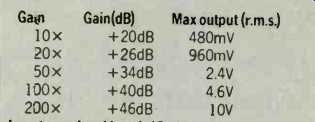
These two values fix a minimum closed loop gain of about 44dB, which is far too high for all but the most insensitive cartridges. The only solution is to use a ladder output attenuator to reduce the overall gain; this would be anathema in a conventional signal path, because of the loss of headroom involved, but since an output of 300mVr.m.s. would be enough to overload virtually all MM inputs, we can afford to be prodigal with it. If the gain of the head amplifier is set to be a convenient 200x ( +46dB) then attenuation to reduce overall gain to a more useful +20dB still allows a maximum output of 480mVr.m.s.; this comfortably exceeds the input capability of the intended host preamplifier, though one previous design would accept it all and come back for more'. Smaller degrees of attenuation to provide intermediate gains allow greater outputs, and these are summarized in the specification. The Ortofon MC 10 was used with +26dB of gain, to give similar output levels to MM cartridges driving the precision preamplifier RIAA stage direct.
The last constraint is the need to provide a low output impedance to the succeeding MM input stage, so that it can give a good noise performance; it is likely to have been optimized to give of its best with a source impedance of 500 ohms or less. This implies that the ladder attenuator will need low resistor values, imposing yet more loading on the unfortunate op-amp, so this problem has been side-stepped by making the ladder an integral part of the AC feedback loop, as shown in Fig.6. This is only practicable because it is known that the load resistance presented by the next stage will be too high at 47 kl2 to cause any significant gain variations.
THE FINAL CIRCUIT
This is shown in Fig. 6, and most closely follows the configuration of Fig.4(d), with the exception that the input devices have suddenly multiplied themselves by three.
Capacitor C1 is soldered on the back of the MC input phono sockets and is intended for r.f. filtering rather than modification of the cartridge response. If the need for more capacitive or resistive loading is felt, then extra components may be freely connected in parallel with R1. If R1 is raised in value, then load resistances of up to 5 kit are possible, as the impedance looking into C2 is about 8kf2. Capacitor C2 is large to give the input devices the full benefit of the low source impedance, and its value should not be altered. Resistors R2,R3 make up DC loop 1, setting the DC operating conditions of Tr1 ,2,3, while R4 is the collector load, decoupled from the supply rail by C9 and R5, which are shared between the two channels. Op-amp IC1 provides the main AC open-loop gain, and is stabilized at h.f. by C4: R6 has no real effect on normal operation, but is included to give IC1 a modicum of negative feedback and hence tidy behavior at power-up, when this would otherwise be lacking due to the charging time of C2, the other op-amp, IC2, is the integrator that makes up DC loop 2, its time-constant carefully chosen to provide plenty of open-loop gain from ICI at low frequencies, and to avoid a peaking in the I.f. response that can occur due to the second time-constant of C2.
The ladder resistors R8-R12 make up the combined feedback-network and output-divider, overall gain being selected by a push-on link in the prototype. A rotary switch could be used instead, but this will produce loud clicks when moved with the volume up, since the emitter current of Tri-Tr;1 flows through R7, and a small current therefore flows down the divider chain.
The output resistor R15 ensures stability when driving long screened cables, and C5 is included to eliminate any trace of DC offset from the output because the stage might find itself driving a horribly vulnerable 'esoteric' input stage with direct coupling and possibly substantial gain at DC Any thing is possible these days.
COMPARING PERFORMANCE PARAMETERS
These are given in the specification, and I think there will be few opportunities to quibble. On the vital question of noise it would be instructive to compare it with other preamplifiers- not easy because the noise performance of MC head amplifiers is specified in so many different ways it is virtually impossible to reduce them all to a similar form, particularly without knowing the spectral distribution of the noise. Noise performances are specified with and without CCIR-ARM weighting, over different band widths, and with different source impedances. This article has dealt throughout with unweighted noise referred to the input, over a 400Hz-30kHz bandwidth, and with RIAA equalization not taken into account.
Without getting bogged down in invidious comparisons, I can only say that it is my belief that the design given here is quieter than most current designs, being within 6dB of the theoretical minimum.
When using this design with the precision preamplifier, it was noted with some surprise that it was so quiet that the MM RIAA stage actually caused the noise performance to deteriorate by about 3dB. Since the RIM stage is itself very quiet (s/n ratio -81dB referred to 5mVr.m.s. input it is considered that the design goals were met.
PRACTICE
PCB layouts require some care if the full performance is to be realised. Firstly, the grounding should be carefully planned, as it must be realised that with such low impedances as R7 (3R3) playing a vital role, the resistance of tracks can be significant. It is suggested that a single star ground point be chosen on the PCB, and critical paths (input ground,R1,R7) all connected to this, to prevent signal currents causing voltage drops where they are least wanted. It is vital to avoid making loops in the input path that will pick up 50Hz magnetic fields.
It is essential to place the decoupling capacitor C8 next to IC1 to prevent insidious h.f. oscillation which makes its presence known only by severely impaired linearity.
When interfacing the head amplifier to an existing design, note that about 8mA flows down the ground connection.
---------
SPECIFICATION
Careful earthing is needed if the noise and crosstalk performance quoted is to be obtained.
Input overload level. 48mVr.m.s.
Equivalent input noise. -139.5 dBu, unweigted, RIAA.
T.h.d. Less than 0.002% at 7Vr.m.s. output,
(maximum gain)at 1 kHz. Less than 0.004%
30hz - 20kHz.
.I
Frrequency response. + 0,- 2dB
20Hz- 20kHz
Crosstalk. Less than -90dB 1 kHz - 20kHz (layout dependent).
Power requirements.
20 mA at + / -15V. for both channels.
References
1. Self, D. "A precision preamplifier", Wireless Work!, October 1983. pp. 31-34.
2. Walker. H.P. "Low-noise audio amplifiers" Wireless World, May 1972.
3. Duncan, B. "AMP-01" HiFi News, October 1984, pp. 67-73.
4. Nordholt & Van Vierzen "Ultra Low Noise Preamp For Moving-Coil Phono Cartridges." JAES. April 1980, pp. 219-223.
5. J. Barleycorn (a.k.a. S. Curtis) HiFi For Plea sure, August 1978. pp. 105-6.
6. A. Foord "Introduction to low-noise amplifier design", Wireless World, April 1981, p71.
7. Self, D. "High-quality preamplifier", Wireless World, February 1979, p40.
(Adapted from: Wireless World magazine, Dec. 1987)
Also see:
- One-Transistor MC Step-up
- Two-Transistor MC Phono Step-up
- Six-Transistor Ultra Low-Noise MC Phono Preamp
= = = =