In our discussion of the composite tele vision signal, carrying amplitude-modulated video information and frequency-modulated sound, it has been shown that a six megacycle wide channel (Figure 137A) is required. Since the television receiver is essentially a high frequency superheterodyne, the major part of the signal amplification and the required selectivity are obtained in the intermediate frequency amplifier system. The television intermediate frequency amplifier system differs in one major respect from the familiar broadcast or short-wave type. The signal which arrives at the grid of the converter consists of two carriers separated by 4.5 megacycles. These two are the video or picture carrier and the audio or sound carrier.

Fig. 184. Block Diagram of a Conventional Dual I -F Channel Television Receiver.
Some method must be provided for separating the information contained in the modulation of these carriers and converting the first to a video voltage at the picture tube grid, and the second to an audio voltage at the grid of the output tube feeding the loudspeaker.
This separation is accomplished in convention al television receivers by providing two intermediate frequency amplifier systems, the first for the video I-F amplification and the second for the audio I-F amplification. (See block diagram of Figure 184.) Since an accurate separation of the two carrier frequencies is provided at the transmitter by "crystal" control, the local oscillator of the receiver, by beating with the composite television signal, automatically produces two intermediate frequencies in the plate circuit of the converter (first detector). The fact that the video carrier and audio carrier are always separated by a fixed difference of 4.5 megacycles, makes possible a very ingenious method of separating the video and audio signals. This system, which is known as "inter-carrier sound", "inter-channel sound", or "carrier difference reception'', was proposed during the war as a means of simplifying military television equipment.
It offers several advantages in the simplification of the television receiver. A block diagram of the "inter-carrier sound" system is shown in Figure 185. In the inter-carrier sound system, the I-F amplifier is made sufficiently broad in response to accept both the video and the audio I-F carriers. At the output of the second detector a new beat note of 4.5 appears between the two signals. This beat is in effect a new intermediate frequency and is frequency-modulated in accordance with the audio signal. It is also amplitude-modulated to some extent by the vi de o or picture signal.
Since the video amplifier is sufficiently wide band in response, this frequency-modulated 4.5 megacycle signal appears in amplified form at the picture tube grid. It is prevented from modulating the picture tube by the use of a trap circuit. The 4. 5 megacycle signal, at the output of the video amplifier, is passed to an F-M detector and audio amplifier. The inter-carrier sound system will be considered in greater detail at the conclusion of our study of video amplifier systems.
Requirements of the I-F amplifier system are similar for either of the two basic systems just described, and are more complex than those encountered in broadcast receiver design.
In abroad cast type super heterodyne receiver, the I-F amplifier need pass a band of frequency extending only 10 kilocycles either side of the center frequency. In F-M receivers the bandwidth need be not more than + or - 200 kilocycles. In a television receiver the intermediate frequency amplifier must pass a band approximately 5 mega-cycles in width.
Coupled with this band pass requirement is the necessity for rejection of interfering signals from the adjacent television channels (see Figure 139).
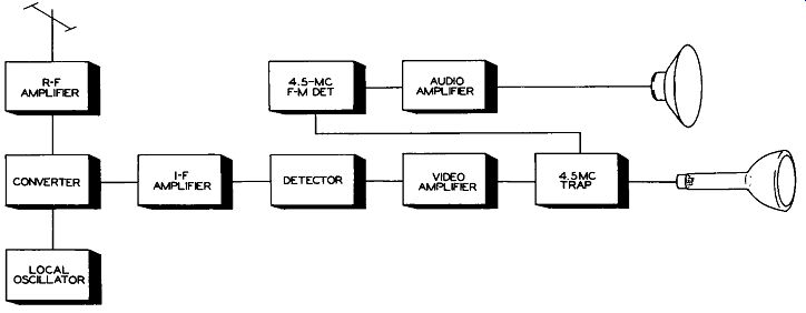
Fig. 185. Block Diagram of an Inter-Carrier Sound Television Receiver.
The factors which influence the choice of I-F frequency are:
1. Bandwidth requirement.
2. Selectivity.
3. Harmonics of the I-F frequency which might occur in a television band.
4. Direct I-F interference. (Signals of I-F frequency passing through the R-F amplifier.)
5. Image rejection due to F-M or tele vision stations on the image frequency.
6. Cross modulation, due to television and F-M stations.
7. Oscillator radiation which will interfere with the operation of other television receivers or F-M receivers in the vicinity.
The choice of any particular intermediate frequency must be a compromise between the various factors just listed, but it appears that the higher intermediate frequencies are a better choice in all respects except direct I -F interference and stage gain.
VIDEO I-F SYSTEMS: The requirements of the video I-F system are fourfold.
1. The bandwidth must be sufficient to accept a total band approximately five mega cycles wide.
2. Frequencies beyond the edges of the pass band must be rejected or attenuated to such an extent that they do not interfere with the picture. These frequencies are:
a. The associated or co-channel sound must be rejected, or reduced to such an extent that "sound bars" do not appear in the picture.
b. The sound carrier of the adjacent, lower-frequency channel (see Figure 139) must be rejected for the same reason.
c. The video carrier, with its modulation, in the next higher adjacent channel must be rejected to prevent an interfering pattern on the picture.
3. The shape of the response characteristic of the video I-F amplifier must be such that the lower frequencies corresponding to the double side-band part of the transmission (Figures 137A and B) are properly attenuated to prevent over-emphasis.

Fig. 186. Output of an Ideal (Linear) Detector when Rectifying the Vestigial
Side-Band Modulated Television Video Carrier.
REQUIRED RESPONSE CHARACTERISTICS OF THE OVERALL VIDEO SYSTEM. An analysis of the transmitter output shown in Figure 137A reveals the fact that the amplitude is constant from the video or picture carrier frequency to a carrier frequency approximately 0.75 megacycles lower and to a frequency of approximately 4 megacycles higher than the center of the video carrier. If such a carrier is impressed on a linear detector, the double side-band nature of the region below the picture carrier will result in an increased output for modulating frequencies extending from zero to 1.25 megacycles. Beyond this point the output will be reduced, since only one side band is employed for frequencies higher than 1.25 megacycles. Figure 186 shows the output of such an ideal detector with an impressed signal from the transmitter modulated by a sweep signal which would produce the envelope of Figure 137A. It will be seen that the output over the region of zero to 0.75 megacycles is twice that of the region from 1.25 megacycles to 4 mega cycles, and that the output drops in an essentially linear fashion from 0.75 megacycles to 1.25 megacycles.
In order to compensate for this increased low frequency output, due to the lower side-band, the overall response curve of the receiver should follow the linear slope of the curve shown as B in Figure 187. This curve passes the 50% response band at the frequency of the video carrier. In actual television receivers we find that the I-F curve is usually of the shape shown as C in Figure 187.

Fig. 187. Overall Receiver Characteristic Required to Compensate for Vestigial
Side-Band Type of Modulation.
As long as the area under the curve to left of the line X-X is equal to the area above the curve to the right of the line X-X, these increments of the video detector output will add to produce the desired curve, D-D. Since the television receiver is normally tuned by means of the sound channel, it is of advantage to have as close an approach to the curve B-B as possible, so the effect of mistuning the video channel will not cause distortion of the low frequency portions of the video modulation, (low frequency "smearing"). The ideal response characteristic for the high frequency end of the band is a sharp cut-off at 4 mega-cycles, shown as curves A and B of Figure 187.
While some receivers do approach this type of curve, most designs provide a more sloping cut-off such as shown by C and D of Figure 187.
While the reduction of high frequencies will result in the loss of some fine detail, when observing a stationary test pattern, this loss is not noticeable if motion occurs in the scene being televised and, in the interest of economy, it has been found possible to reduce the pass band to 3 megacycles without noticeable degradation of the picture.
Up to this point our discussion of the position in the television channel of the video and sound carriers, as well as the adjacent channel frequency, has been concerned with their position in the spectrum as transmitted R-F signals. Since the local, or beating, oscillator of the television receiver is positioned at a frequency higher than the signal, all of these frequencies will be inverted in position when they appear as intermediate frequencies in the detector output. Figure 188 shows, in chart form, the various channel frequencies, video and audio carriers, local oscillator frequencies and I-F frequencies, of a typical television receiver.

Fig. 188. Chart of Typical Frequencies for the Local Oscillator and I -F Amplifiers
of a Television Receiver.

Fig. 189. Overall Video I-F Response Curve Showing Location of I-F Trap
Frequencies.
Figure 189 shows the overall video I-F response curve for the receiver employing the frequency compensations of Figure 188. On this curve are shown not only the significant I-F frequencies of the desired channel, but also the position of adjacent channel frequencies which might interfere with the operation of the receiver. The curve is seen to be depressed at these points. This reduction in response is accomplished by means of "trap" circuits.
With regard to the choice of an intermediate frequency for television, it should be noted that a number of limitations are set by standards of the television system and frequency assignments. The I-F frequency chosen must lie between the highest video frequency component on the one side and the lowest television frequency channel assignment on the other. This means that television I-F frequencies cannot be lower than approximately 8 megacycles nor higher than 50 megacycles.
Figure 190 lists the video and audio I-F frequencies which have been employed in commercial television receivers in the post war period. The present design trend indicates that the higher frequencies may be chosen as the eventual standard for television receivers.
Industry standardization committees are considering possible advantages of frequencies as high as 45.7 megacycles for video I-F, which would necessitate the use of 41.2 megacycles for the audio I-F.

Fig. 190. Television Intermediate Amplifier Frequencies in Commercial Use.
METHODS OF OBTAINING WIDE BAND RESPONSE REQUIRED FOR VIDEO I-F. There are many types of coupling networks which can be used between the amplifier tube s of the video I-F amplifier to accomplish the wide band response required. Three major methods are currently used in receiver design. These are:
1. Over -coupled transformers with shunt resistance loading.
2. Staggered-tuned circuits.
3. Pairs of single-tuned circuits with overall negative feedback.
Of these systems, the second (or staggered-tuned circuit) is the most popular. The performance of the various types will be described and illustrated by typical examples later in this section. The circuits employed to reject undesired responses will be described separately from the coupled means used to assure a wide pass band.
Video I-F Amplifiers with Over-Coupled Tuned Transformers: If "an interstage tra US: former with primary and secondary tuned to the same frequency has the coupling between the circuits progressively increased, a "double-humped" resonance curve will result after a point known as "critical coupling" has been passed. These double humps can be "smoothed" to a flat-top response curve by load in g the primary and secondary circuits with the correct values of resistance. This of course results in lower Q and consequently lower gain than would be obtained with a narrower passband . Figure 191 shows an intermediate frequency amplifier system using over-coupled transformers. The placement of parts of this system are shown in Figure 192.
The amplifier of Figure 192 makes use of three band-pass coupled stages employing type 6AU6 miniature tubes. Transformers L3-L4, L7-L8, L10-L11, and L12 -L13 are over-coupled, and are then loaded with resistance in the secondary circuits to produce the flat-top band-pass characteristic. Although no primary shunt resistance is shown except in the case of coil L3, the plate-to-cathode resistance of the tubes provides the required primary loading. Broad tuning of the primary circuits is accomplished by the output capacitance of the stage and the associated wiring. No tuning adjustment is provided in the primary circuits with the exception of the last transformer (L12--L13).

Fig. 191. Video I -F Amplifier Employing Over-Coupled Transformers.

Fig. 192. I-F Amplifier Inductances of Figure 191. Photo from Sample Receiver
Courtesy General Electric Company Winding L5 of the input circuit of the amplifier
tube T2 connects to a series -tuned trap, consisting of L5, L6 and capacitors
C9 and C10 in parallel. This network is used to adjust the slope of the curve
at the high frequency end of the I-F band. This is the section of the curve
which is essentially double side band (due to vestigial side-band modulation).
While viewing the response curve on an oscilloscope, the tele vision service
technician can adjust capacitor C10 to place the 50% response point at the
position of the video I-F carrier (26.3 mega-cycles in this particular receiver).
The series-tuned trap circuit, consisting of coupling capacitor C15 with tuned
circuit elements L9 and C16, is adjusted to reduce or attenuate the sound
carrier of the channel being tuned (21.8 megacycles). A tap on inductor L9
provides the audio intermediate frequency voltage for amplification by a second
I -F amplifier system. At the frequency of series resonance of this circuit
(21.8 megacycles), it effectively shunts the grid circuit by a low impedance,
which puts a "notch" in the response curve of the amplifier.
Video I-F Amplifiers with Staggered Tuned Circuits. Another solution to the problem of designing a video intermediate frequency amplifier to meet the requirements discussed, is that of coupling the tubes by single-tuned circuits which are tuned to different frequencies within the desired pass band.
If a number of single-tuned circuits (between amplifier tubes) are all tuned to the same frequency, the bandwidth decreases as stages are added, and the overall response grows more "peaked" or selective. However, if the tuning of the individual circuits are "staggered" about the center frequency, and the Q values of the circuits are adjusted by proper shunt resistor loading, the desired bandwidth c an be obtained and a very satisfactory overall curve shape will result.
Curves B and C of Figure 193 illustrate the effects of the frequency of tune on the band width of a pair of identical circuits (Figure 193A) as discussed above, first to the same frequency and then to frequencies separated from the center frequency by half of the band width of the individual circuits. The bandwidth of a circuit is defined as the frequency "spread" between the points on the resonance curve at which the response is . 7 of that at resonance.

Fig. 193. An I -F Amplifier Stage employing Single Circuit Impedance Coupling.
B Effect of Tuning the Circuits of Amplifier to the same Frequency. C Effect
of “Stagger-Tuning'' the Frequencies of Amplifier A .
When both circuits are tuned to the same frequency as shown in Figure 193B, the overall bandwidth of the amplifier (Figure 193A) will be 64 percent of the bandwidth of the individual circuit. If, on the other hand, the tuning of the individual circuits is ''staggered" above and below the center frequency as in Figure 193C, the overall bandwidth becomes 40% greater than that of the individual circuits.
While we have used the case of two circuits to explain the effects of stagger-tuning, the practical television video amplifier involves the staggering of more circuits to achieve the 4 to 6 megacycle bandwidth required. In the case of the two circuits just illustrated, the individual bandwidths and circuit Q values have been made identical for the sake of simplicity.
In the actual circuits employed in television receivers, the circuit Q values are varied to produce resonance curve shapes and stage gains which will in turn cascade to produce the overall curve shape of Figure 189.
Figures 194, 195, 196 and 197 illustrate the details of a stagger-tuned video I -F amplifier system which is typical of many receiver designs in use.
Figure 194 shows the individual resonance curves of the various coupling circuits. Four stages of video I-F amplification are required to obtain sufficient I-F gain, and the necessary wide band characteristic. The effective Q of each circuit is determined by either the shunt plate resistance or a grid circuit resist or, so that the response curves produce the desired overall response shown by the dotted line of Figure 194. It will be noted that circuits 7 and 3 are high Q, circuits 5 and 6 of lower Q, and that circuit 9 of lowest Q is used to "fill" in the center of the curve.
In a stagger -tuned system variations of the individual amplifier tube gains do not affect the shape of the response curve and thus the amplifier is not unduly sensitive to tube interchange.

Fig. 194. An Example of a "Stagger-Tuned" Video I-F System.

Fig. 195. The Effect of Cascading the "Stagger-Tuned" Circuits of
Figure 194.

Fig. 196. Video Coupling Coils Used in the Video I -F Amplifier of Figure
195. Photo from Samples Courtesy F. W. Sickles Co.

Fig. 197. Video and Audio- I-F System of Figures 194, 195, and 196. Photo
from Sample Receiver Courtesy R. C. A.

Fig. 198. Another Example of a "Stagger-Tuned" Video I-F Amplifier.
Figure 196 shows the various coupling units employed in this circuit identified by symbol numbers as to circuit position in the schematic of Figure 194. The converter plate unit (L1-L2) and the coupling unit between the second and third stages (L8-L9) are shown as used and also in disassembled form.
One of the advantages of the stagger-tuned amplifier is the fact that stability or freedom from a tendency · to regenerate or oscillate is provided by the fact that grid and plate circuits of each amplifier tube are tuned to different frequencies. This makes it possible to construct the amplifier with a minimum of shielding. Figure 197 shows the corner of the chassis employing the circuit of Figure 194.
It will be seen that the only shield employed is that surrounding circuit number 8. This circuit (sound trap for the accompanying sound I-F) is tuned to the s am e frequency as circuit 2 (L2--C4). overall oscillation by magnetic coupling would occur if it were not shielded.
Another important feature of stagger tuning is the fact that alignment can be accomplished by a signal generator set to each of the individual circuit frequencies, while using a VTVM at the video detector for output indication. A sweep generator and oscilloscope are required for observation of the overall curve only.
The ''trap" circuits, employed to reduce the response of the amplifier at the frequencies corresponding to the adjacent higher channel video carrier, the accompanying sound carrier, and the next lower adjacent channel sound carrier, have been indicated in Figure 194 and will be explained in detail later in this section.
Another example of a stagger-tuned video amplifier is shown in Figures 198, 199 and 200. In this case the entire video I-F amplifier, video detector, video amplifier and video output tube have been constructed as a strip sub assembly. This unit is available for the assembly of television receivers by experimenters and students. Figure 198 shows the schematic wiring diagram of the unit which is illustrated photographically in Figures 198 A and 198B. In this case the same principle of stagger -tuning is employed with the exception of the fact that different frequencies have been chosen to produce the required wideband...

Fig. 199. Top View of Amplifier Shown in Figure 198. B Bottom View of Amplifier
(Figure 198. Photo from Sample )

Fig. 200. Coupling Units Used in Amplifier (Figure 199). Photo from Sample
Courtesy Meissner Mfg. Div., Maguire Industries, Inc. Meissaer Mfg. Div., Maguire
Industries, Inc.
... curve. Absorption type traps are used to reduce the co-channel and adjacent channel interference. The coupling units are placed in individually shielded containers which make possible a very compact design. Figure 199B shows the bottom view of this assembly.
A unique feature of the design is the use of a germanium crystal as the video detector.
It is housed within the shield compartment of the final coupling unit, L7. The details of construction of an interstage assembly (L5, L16, C13, C14, R16) and the output-detector stage R1 7, C1 7, L7, L8 and R18 are shown in Figure 200. The balance of the video system shown on the strip will be described when we consider in detail, the subject of the video amplification.
Wide Band Video I-F Amplification
Employing Negative Feedback, another method for obtaining wide band response with simplified alignment procedure is the use of negative feedback or degeneration around an amplifier stage comprised of input and output tuned circuits. Amplifiers of this type were employed in the intermediate frequency section of radar equipment during the war and are currently under consideration for television use. A four stage amplifier is shown in Figure 201. The coupling between tubes consists of a variable conductor (L 1, L3, or L5) with the associated interelectrode tube and circuit capacitances. Resistors R3 and R15 connected from plate to grid of tubes T2 and T4 respectively, apply feedback voltage which results in broadening the bandwidth of the amplifier.
An amplifier of this type can be aligned by disconnecting one end of each of the feedback resistors, and then tuning all of the circuits to the center frequency, taking into account the slight change of capacity caused by removal of the resistor (approximately .3mmf). Since a change in the gain of the degenerated stage would result in a change of the bandwidth of the stage, it is possible to apply gain control to tubes R1 and T3 only. These tubes are not involved in the degeneration.
For simplicity, trap circuits for the reduction of undesired responses have not been included in this diagram.

Fig. 201. A Video I-F Amplifier Employing Negative Feedback for Band Widening.
REJECTION OF UNDESIRED ADJACENT CHANNEL AND CO-CHANNEL CARRIERS. In our consideration of the required response curve shape of the video I-F amplifier (see Figure 189) we have seen the necessity of reducing the response at the position which would be occupied by the sound carrier of the same channel being received, the video carrier of the next higher adjacent channel, and the sound carrier of the next lower adjacent channel.
The production of low response points or "notches" at the I-F frequencies corresponding to these carriers can be accomplished in the video amplifier by one or a combination of the following circuits:
1. Series-tuned circuit traps.
2. Parallel-tuned circuit "absorption" traps.
3. Cathode circuit or degenerative traps.
4. Bridged T networks as coupling elements and rejection circuits.
The trap circuits, items 1 and 2 (series and parallel tuned), are similar in function of operation to interference elimination traps which have been used in the radio service profession for the elimination of image interference or interference by strong local stations. The degenerative trap principle is often used in audio circuits for compensation, while the fourth or bridged T type of trap is similar in action to a null bridge, such as is employed for measurement purposes.
Series-Tuned Trails. The series-tuned trap is the acceptance type and acts as a virtual short circuit across the system at its frequency of resonance. The impedance at this frequency is very low and is equal to the AC resistance of the circuit components. In the amplifier shown in Figure 191, the circuit comprising L5 and L6 in series, tuned by capacitors C9 and C 10 in parallel, is used to adjust the slope of the high frequency end of the band pass curve. It permits the control of the point at which the video carrier falls (50% of maximum response for compensation of vestigial side-band effect). When this adjustment is made the curve falls off at a sufficient rate to reject the next lower channel sound carrier also. In this case the adjacent sound carrier falls at 27.8 megacycles. This series tuned circuit is coupled to the secondary circuit (L4) by means of the coupling coil (L5). In the grid circuit of the second video stage of this same amplifier (Figure 191) will be found another series -tuned trap. In this case, C15 and the parallel combination of L9 and Cl6, are tuned for maximum attenuation at 21.8 megacycles which is the associated or co-channel sound I-F carrier. It is necessary to reject this carrier from the video amplifier to prevent the production of "sound bands" on the picture. The trap serves the dual purpose of rejecting the sound channel and at the same time providing a resonant pick-off of the sound or audio I -F voltage for amplification through an audio I-F amplifier.
Shunt-Tuned or Absorption Type Traps.
The absorption type trap is the most frequently used type of rejection circuit for undesired responses. Three traps of this type are shown in the schematic diagram of Figure 194 (circuits 2, 4 and 6). They consist of a parallel-tuned circuit coupled to the plate load of the video I-F stage. At the frequency of resonance of the circuit, a high circulating current is developed in the trap. The trap reacts through its inductive coupling in such a manner as to reduce the load impedance of the stage and greatly decrease the amplification at the point of tune. The effects of trap circuits 2, 4 and 6, of Figure 191, on the response curve of the amplifier are shown in the correspondingly numbered points on the overall amplifier curve of Figure 189.
Cathode Circuit or Degenerative Traps.
Another method employed to reduce the amplifier gain at a particular point, is to use selective degeneration. This is done by placing a parallel resonant circuit in the cathode-to-ground circuit of one of the amplifier stages. This may be done either directly in the cathode circuit, or by coupling to it. At the resonant frequency of the trap, a high impedance appears in the circuit and the trap acts like a large un-bypassed resistor, causing degeneration and reducing the amplification of the stage to a very low value. The rejection figure of such a degenerative trap never can be greater than the gain of the stage, which in the case illustrated is approximately eight to one.
To prevent degeneration at the frequency of tune, or 25.2 megacycles, the primary coil L 12 has been made broadly series-resonant at this frequency by means of tuning capacitor C25. This makes the cathode impedance low at 21.25 megacycles and prevents a loss in gain.
Figure 202 shows the use of a network of circuit elements known as the "bridged T". These circuits, for rejection of the undesired associated sound and adjacent sound I -F carriers, use a T-shaped branch consisting of two capacitors and a resistor (C13, C14--R12) and (C18, C19--R19) "bridged" by an inductor (L5 and L13 respectively). The I-F amplifier shown in the photograph of Figure 203, uses the schematic of Figure 202.

Fig. 202. A Video I-F System Using "Bridged T" Networks as Interference
Traps.

Fig. 203. Video I-F System Shown in Schematic (Figure 201). Photo from Sample
Receiver Courtesy Philco Corporation.

Fig. 204. Diode Video Detector Output Polarity.
The action of this arrangement is equivalent to a bridge circuit, but has the ad vantage that the input and output circuits can have a common terminal at ground potential.
The conditions of balance (for a null or low output) occur when the reactance of the variable inductance is made equal to the reactance of capacitors in series, and when the resistor in the center leg of the T is approximately one fourth of the parallel resistance of the tuned circuit. Another explanation of the circuit is that of an anti-resonant trap in the line with a secondary balance for the resistance losses of the circuit. Much sharper null "notches" and greater degree of rejection can be obtained by the use of the bridged T connection than with the trap circuit alone.
Over the video I-F band (22.6mhz to 28mhz in the example of Figure 202) trap circuit, which is tuned to a frequency lower than the band, acts as a capacitance coupling unit between the two stagger-tuned circuits, and circuit 2, tuned above the band, acts as an inductive coupling element.
Another variation of the bridged T circuit (not illustrated) em ploys a center -tapped coil for the resistance branch and a single trimmer for the capacitance branch.
VIDEO DETECTORS. The video detector which follows the video I-F amplifier just discussed, is essentially the s am e type of demodulator as is used for the second detector of an A-M broadcast or short wave radio receiver. The only significant circuit differences between a video second detector and the familiar A-M second detector resides in the fact that the polarity of its output must be taken into consideration and compensation must be employed to prevent loss of the higher video frequencies.
Since the system of television broadcasting, in use in this country, is based on negative video modulation, the detector output must be of such polarity that an increase of carrier strength causes the video voltage at the picture tube control grid to become more negative and thus decrease the brilliance of the picture element.
If there are an eve n number of video amplifying stages between the detector and the picture tube grid, the output of the detector must be "negative going". In other words, an increase in I-F carrier strength, applied to the detector, results in a more negative video signal with respect to ground. Figure 204A shows a detector which supplies a negative picture polarity followed by two video stages.
If an odd number of stages are employed (in most instances this will be a single stage), a detector must be connected as shown in Figure 204B. This circuit, with the plate of the diode connected to the high side of the video coupling circuit, produces a video output across the load resistor which increases in positive polarity as the video carrier strength is increased.

Fig. 205. Video Detector of Negative Polarity Feeding Picture Tube Grid through
Two Video Stages.

Fig. 206. Video Detector of Positive Polarity Feeding Picture Tube Grid through
a Single Video Stage.
A typical video detection and amplifying system which employs negative polarity video signal from the diode is shown in Figure 205.
In this case the load resistor (R2) has a value of 3900 ohms, and has associated with it a group of circuit elements, C3, L3, L4, and R1, whose purpose is to assist in producing a flat video response characteristic over a range of from 30 cycles to more than 4 megacycles.
A significant difference between the operation of the diode as an A-M detector and as a video detector lies in the value of the load resistor. In the familiar broadcast application, a typical diode load varies from .5 to 2 megohms, and maintains this high load resistance over the range of frequencies required for sound reproduction. In most instances this involves frequencies no higher than 5000 cycles. In the video detection case, however, the capacitance of the diode and the capacitance to ground of its associated circuit prevent the use of a high diode load resistance, since it is necessary to provide flat response to at least 4 megacycles. At these high frequencies, the reactance of the circuit and tube capacitance would become lower than the load resistance, and thus by-pass the high frequencies. For this reason, the load resistance is made of the low value and the compensating elements just discussed produce a resonant rise of circuit impedance at the high end of the video band.
L3 is called a series-peaking choke, and L4 a shunt-peaking choke. These compensating elements are employed in each video stage (L5-L6, L7-L5, of Figure 205). A more complete discussion of their function will be presented when the subject of video amplification is considered.

Fig. 207. A Positive Output Detector Feeding the Cathode of the Picture Tube
through a DC Amplifier.
Figure 206 shows a video detection and amplification system which employs the diode with its plate connected to the high side of the I-F input circuit in order to produce a "positive-going" video signal. In this case a single video amplifier stage is used, inverting the polarity, thus producing a more negative voltage at the picture tube control grid as the carrier strength increases. A combination of L3 and C4, together with the circuit capacitances, resonates at the high end of the video band and maintains a flat response from the detector. Choke L3 also serves to reduce the 4.5 megacycle beat which occurs due to the associated sound I-F carrier beating with the video carrier. The presence of this 4.5 mega-cycle video interference would reduce the fine detail of the picture.
In the foregoing discussion, as illustrated by the circuits of Figures 205 and 206, the video output tube is coupled to the control grid of the picture tube. In certain television de signs, for reasons of circuit simplification, the input to the picture tube is inverted and the plate of the video output tube is coupled to the cathode rather than to the control grid. When this is done, in order to turn over the signal at the picture tube input, it is necessary to reverse the rule previously stated and employ a positive rather than a negative-going signal for an even number of video stages. Figure 207 shows an example of such a circuit which employs the negative output detector ( T1) with a single stage amplifier (T2) feeding the cathode of the picture tube (T3). A novel feature of this circuit, to be discussed in greater detail later, is the fact that the output of the detector is "direct-coupled" through the entire video amplifier to the picture tube. No coup ling or blocking capacitors are employed and the diode ( T1) therefore can fulfill the dual roles of detection and DC re-insertion.
THE GERMANIUM CRYSTAL DIODE AS A VIDEO DETECTOR. The small, cartridge type, fixed crystal rectifiers (see Figure 208) which were developed during World War II for radar converters are finding applications in television design as a substitute for a thermionic diode. The germanium type (1N34) is being employed not only as a video detector but also as a DC restorer or DC re-insertion diode.
Figure 209 shows two typical applications of crystal detectors as vi de o demodulators.
Figure 209A shows a load circuit, consisting of resistor R5 and high frequency compensation network C4, L2, L3 and R4, connected in series with the diode. Figure 209B shows a shunt connection of similar elements.
Several features of the germanium crystal diode recommend its use as compared with the vacuum tube type. These are: lower capacitance , smaller size, lower dynamic resistance, reduction of power consumption (no heater required) and ease of mounting (no socket required). The lower capacitance and materially lower dynamic resistance result in improved performance as a video detector by providing higher rectification efficiency for a given bandwidth. Its improved linearity at low signal levels helps preserve highlight detail in the picture.

Fig. 208. Germanium Crystal Diode Type 1N34. Photo from Sample Courtesy Sylvania
Electric Products, Inc. (For service the 1N34 can be used to replace the 1N36.
The 1N34 has a higher voltage rating.)

Fig. 209. The Germanium Crystal as a Video Detector.
AUDIO IF SYSTEMS: The audio IF system of the television receiver is similar in design to the IF system of the conventional FM receiver.
Two major differences from the standard FM set will be noted:
1. The intermediate frequency which has become standard for FM broadcast receivers is 10.7 mhz. No standard is yet apparent for television audio IF frequency. This value is automatically established by the choice of video IF frequency (a difference of 4-1/2 mhz exists between the video IF frequency and the audio IF frequency).
2. The deviation of the television sound carrier for maximum modulation has been established as 25khz (a tot al sweep of 50khz), whereas the maximum deviation for standard FM broadcasting has been set at 75khz (a maximum sweep of 150khz). The fact that a lower deviation is employed for television sound would indicate the possibility of using a narrower pass band for the audio IF channel and a shorter linear region for the second detector or discriminator. The pas s band of the IF amplifier is kept at several hundred khz and the linear region of detection extended to the same figure. This audio IF pass band is required to r ender the receiver operation immune from frequency drift. An extremely small percent age drift of frequency of the local oscillator would be sufficient to move the audio IF frequency out of the pass band if it were made only wide enough to accommodate the 50khz sweep. This small drift would not disturb the quality of the picture due to the vestigial side band nature of the video signal. In the inter-carrier sound receiver system, to be described in detail later, a drift of the sound IF frequencies (4.5mhz) is not possible. The difference between the video and audio carriers is established by crystal control at the transmitter. A wide pass band is employed, however, since any drift of tune of the IF amplifier cannot be corrected by receiver tuning, and some tolerance must be provided for such a condition.

Fig. 210. Methods of Separating the Audio IF from the Composite IF Signal.
METHOD OF AUDIO IF "TAKE-OFF". In the conventional dual IF channel television receiver (Figure 184) two separate intermediate frequencies exist in the output of the converter. We have considered the nature of the composite IF signal and have indicated in various schematic dia grams (Figures 191, 194, 198 and 202), the points at which the audio IF is taken from the composite signal and passed on to the audio IF system.

Fig. 211. A Typical Audio IF System. Illustrated in Figure 197.
Figure 210 shows in simplified form, the various circuits employed for separation or "take -off" of the audio IF signal. In each instance the take-off circuit serves the dual purpose of providing a resonant system for the development of audio IF voltage, and a trap circuit to prevent this audio IF voltage from progressing further through the video IF amplifier to produce interference in the picture.
The point in the video IF amplifier system at which the audio IF is separated, is determined by considerations of bandwidth and total gain required to produce an adequate signal at the sound detector or discriminator.
In many receivers, audio IF separation is accomplished in the converter plate circuit as shown in Figures 194 and 198. In other receivers, one or more video amplifier stages are interposed between the converter and the sound take -off point. Such amplifier stages must have a sufficiently wide pass band to accept both the video IF signal and the audio IF signal. A total bandwidth of approximately 5mhz is required for these stages. Examples of audio IF take -off following several stages of combined video and audio IF amplification will be found in Figures 191 and 202.
Figure 210A shows a combination audio IF absorption trap and sound take-off. The audio IF grid is "tapped down" on the circuit in order to preserve high circuit Q for rejection, since the grid loading would normally reduce the Q, and thus the effectiveness of the circuit as a trap. The construction of the transformer L 1--L2, of Figure 210A is shown in Figure 194.
In Figure 210B, the combined trap and take-off circuit L4-C3 is capacitance-coupled to the video amplifier interstage circuit by means of capacitor C2, and thus acts as a shunt acceptance circuit.
Figure 210C shows the use of the bridged T network as explained.
In this case, the entire video and audio IF signal appears across L 1,and is passed through C1 to the audio IF amplifier. Selection of the audio IF portion is accomplished by the tuned circuits which follow. The audio IF signal is prevented from reaching the balance of the video IF amplifier by the action of the trap circuit consisting of L2, C3, C4 and R1.

Fig. 213. Another Example of a Television Audio IF Channel.
Figure 210D shows the degenerative cathode trap circuit, discussed, as a sound take-off. In this case, the vi de o IF amplifier tube serves as a cathode follower type of stage, as far as the audio IF signal is concerned. The stage acts as a cathode loaded amplifier at the frequency of the audio IF, due to the tuned circuit (L2-C2) in the cathode return. Because of this tuned cathode load, the audio IF is degenerated as far as the plate ........ circuit is concerned, and very little voltage appears for amplification by the succeeding video IF amplifying stages.

Fig. 212. IF Transformers Used in the Circuit of Figure 211.
TYPICAL AUDIO IF SYSTEMS. Figure 211 shows, in schematic. form, the audio IF system which is the companion of the video IF circuit of Figure 194. The transformers employed are shown in Figure 212. Interstage transformers, L4-L5, and L6-L7, are over coupled, with a center frequency of 21.25mhz.
The third stage (tube T4) acts as a limiter.
Circuit R8-C15 in the grid return, provides a bias by grid rectification of the signal to clip one side of the IF envelope by plate current cut-off. The plate and screen run at low voltage (48 volts) as established by the divider comprised of resistors R9 and R10. This provides clipping of the operation beyond the "knee" of the plate voltage-plate current characteristic (the saturation region). The discriminator is seen to be of the familiar Foster-Seeley type.
Another typical audio IF system is shown in the circuit of Figure 213 and the photographs of Figures 214A and B. Again we find the use of over-coupled transformers, a limiting stage and an FM discriminator. The discriminator network is somewhat unconventional and will be described in greater detail under "Variations of the Foster-Seeley circuit". In this amplifier, limiting is accomplished in both the second and third stages by circuits of widely differing time constants. The circuit of Figure 213 and the amplifier strip of 214 are companions to those of Figures 198 and 199 respectively.
Due to the fact that audio IF systems employed in television are identical in type to those employed in standard FM receivers, no detailed theory of their operation will be given here. Many excellent explanations are to be found in current books and magazine articles available to the service technician.
Television sound differs from the standard FM transmission in deviation. Wideband (75khz) deviation is superior in noise reduction to television (25khz) deviation. Both are capable of the same fidelity and volume range.
THE FOOTER-SEELEY FM DISCRIMINATOR AND ITS VARIATIONS IN TELEVISION SOUND SYSTEMS. At least three basically different types of FM demodulation circuits are employed in FM broadcast receivers, namely: the Foster -Seeley discriminator, the ratio detector and the locked oscillator. Of these only the first two types have been employed to date in television receivers.

Fig. 214. The Television Audio IF Channel of Figure 213. (A) Top View. B.
Bottom View.
A. BASIC FOSTER-SEELEY DISCRIMINATOR; B. VARIATIONS OF THE BASIC DISCRIMINATOR

Fig. 215. The Basic "Foster-Seeley" Discriminator and the Variations
Employed in TV Receivers.
The Foster -Seeley discriminator shown in Figure 215A is familiar to the television service engineer, not only as an FM detector but also as a method of obtaining a control voltage for A. F. C. systems (see flywheel or A. F. C. horizontal scanning control, control of the local oscillator of the RF system).
The discriminator of Figure 215A provides an audio output which, at any instant, is equal to the difference between the rectified output of diode T2 (across R4) and that of diode T3 (across R5). The IF input is applied to the diodes by the circuit consisting of the tuned IF transformer L 1-L2,C3 -C6 and in-phase network C5-L3 with bypass capacitors C7 and ca. The action of this system is to combine the output of the transformer, which is supplied to the diode plates 180° out-of-phase with a 90° or quadrature component. As the frequency shifts either side of the IF center frequency, the instantaneous voltage on one diode will increase as that on the other decreases. This results in the production of both DC and audio voltages across the series combination of load resistors R4 and R5.
This type of FM detector will discriminate against amplitude change only at its center tune or zero modulation frequency. For this reason it is usually preceded by a limiting stage as described.
To improve the signal to noise ratio, it is standard practice to "pre-emphasize" the high frequency portion of the audio signal in the modulation of the television transmitter.
This "pre-emphasis" is corrected in the receiver by a "de-emphasis" circuit consisting of a series resistor and shunt capacitor (R6 and C9 of Figure 215A). The time constant of this combination is fixed at 75 micro-seconds to conform to the FCC standard.
Several variations of the basic discriminator, in current use, are illustrated in Figure 215B. In Figure 215B-1, the resistor R2 replaces the reactor L3 of Figure 215A. Figure 215B-2 eliminates both the choke and the resistor of the preceding circuit by introducing the quadrature component at the junction of the audio load resistors R2 and R3, the resist ors being bypassed by a single capacitor C5.
Figure 215B-3 shows another method of introducing the quadrature voltage . In this case, the tuning capacitance for the transformer secondary consists of two equal capacitors,C3 and C4. The voltage fed from the plate of the limiter is thus coupled to the diode plates "in-phase" and of equal amplitude. To complete the DC return paths of the diodes, resist ors R2 and R3 have been added to the circuit.
Figure 215B-4 illustrates a method of using a duo-diode tube with a common cathode in a discriminator circuit. To accomplish this, the secondary of the input transformer has been constructed in two halves with the diode loads in series in the individual plate-to-cathode paths.
RATIO DETECTORS. The ratio detector is a popular type of FM demodulator in tele vision receivers. Several features distinguish it from other types of FM detectors. These are: an inherent rejection of amplitude modulation, and the ability to provide an automatic volume control voltage proportional to the peak value of the audio IF carrier.
Figure 216A shows the basic ratio detector circuit. The input network is identical to that of the basic Foster-Seeley discriminator of Figure 215A. The resemblance stops at this point because the diodes are arranged in series or additive fashion rather than in opposition to one another as in the discriminator. Another difference which is significant is the use of an electrolytic capacitor C10 across the diodes and load resistors.
The electrolytic capacitor is charged, through the diodes, by rectification of the applied IF carrier. The time constant of C10 and the series combination of R4 and R5 is approximately a quarter of a second. The bias voltage from this circuit "clamps" the diode conduction level at a value determined by the applied carrier. An instantaneous change, such as might be caused by a burst of noise, cannot change this bias due to the long time constant of the circuit. For the same reason, the total audio voltage across the series capacitors CS and C9 is held constant. Any change in output of either diode, caused by a shift of frequency will thus cause the ratio of voltages across the capacitors to change, but will not change their sum. Thus the detector output is proportional to the ratio of IF voltages on the diodes, and not to the difference between these voltages.
Due to its insensitivity to amplitude modulation, the ratio detector does not require a preceding limiter and the last audio IF stage can be run at full voltage and gain.
Figure 216B shows several variations of the basic type of ratio detector.
In Figure 216B-1, the major difference is the use of a close coupled winding L2 to supply the quadrature voltage.
Figures 216A, 216B-1, 3 and 4, are of the balanced type, i.e., the circuit is balanced with respect to ground. Figure 216B-2 is known as the unbalanced type. In this case, one end of the electrolytic capacitor is grounded, as well as its shunt resistor R1. The IF path, which supplies diode T1, is completed by the bypass capacitor C4. The capacitor C6 is made variable to take care of stray circuit capacitance balance.

Fig. 216. The Ratio Detector for FM Demodulation and its Variations Employed
in Television. A. BASIC RATIO DETECTOR CIRCUIT; B. VARIATIONS OF THE BASIC
RATIO DETECTOR CIRCUIT
Figures 216B-3 and B-4, both illustrate expedients employed to assure a condition of equal diode inputs at the zero modulation or IF carrier frequency. In Figure 216B-3, separate shielding of portions of the input circuit has been provided to reduce unbalanced coup ling. Figure 216B-4 illustrates the ratio detector circuit used to provide an A. F. C. voltage for automatic control of the RF local oscillator, shown in Figure 179. An accurate balance for the carrier tune point is assured by the use of trimming capacitor C4. A small capacitor C3 (5 mmf.) has been added, between the top of the circuit and ground, to assure that the balance point will be within the range of the trimmer C4.
While the ratio detector can provide an A.V.C. voltage for IF amplifier control, this is normally not utilized. A.G.C. from the video system usually provides this function.
The television sound signal is employed as a means of fine tuning the receiver for both sound and picture, since a drift of tune which would distort or lose the sound, would cause very little change of picture contrast or detail.
It is important however, that the audio IF system and the alignment of the detector be centered at the correct intermediate frequency which differs by exactly 4.5 megacycles from the video IF carrier frequency. When the receiver is so tuned, the extra bandwidth allows additional latitude for oscillator drift.