The output of the video detector seldom exceeds a few volts and s inc e the picture tube requires a grid swing of approximately 40 volts (see Figure 110), for its range of black to white, it is necessary to amplify the signal through one or more stages of video amplification.
In our study of the nature of the video modulating signal, we have seen that the range of frequencies encountered extends from 30 cycles to over four million cycles per second. The design of an amplifier to provide uniform gain over this extended band, involves the use of compensating circuits and pentode amplifying tubes of high transconductance. The basic circuit, to which correction networks are applied, is the familiar resistance and capacitance-coupled audio amplifier.
Figure 217 A shows a typical pentode amplifier with its coupling elements, and with the inter-electrode capacitance of the tubes indicated in dotted lines. When employed in a conventional broadcast receiver, the solid line curve of Figure 217B would represent a gain versus frequency characteristic which would be entirely adequate for sound reproduction.
The dotted line of Figure 217B shows the required gain characteristic of an amplifier for the video band of frequencies.
For purposes of analysis, the effect of the circuit elements on the frequency characteristic can be represented as shown in Figure 218. The equivalent circuit of the amplifier at all frequencies is shown by the network of Figure 218A. This network has been re-drawn at B, C, and D to represent the equivalent circuits at low, medium and high frequencies.
These ranges correspond respectively to the regions 1, 2, and 3, of Figure 217B.
A. TYPICAL RESISTANCE COUPLED AUDIO AMPLIFIER STAGE
B. REQUIRED VIDEO BANDWIDTH COMPARED WITH TYPICAL AUDIO BANDWIDTH
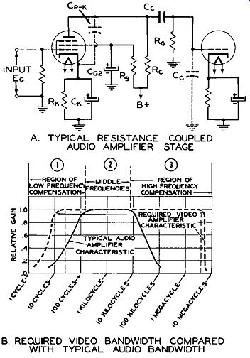
Fig. 217. Response Requirements of Video Versus Audio Amplifiers.

Fig. 218. Equivalent Circuits of Resistance-Coupled Stage at Low, Middle and
High Frequencies.
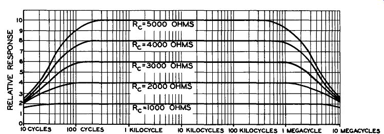
Fig. 219. Effect of Plate Coupling Resistor on Gain and Bandwidth.
Three separate expedients are employed to extend the range of a resistance and capacitance-coupled amplifier for video use. These are:
1. The use of low values of plate load or coupling resistance R_c in conjunction with high trans-conductance tubes.
2. Low frequency compensation for the effects of the coupling network Cc-Rg-
3. High frequency compensation for the effects of total circuit capacitance Cs.
EFFECT OF THE PLATE LOAD RESISTOR ON BANDWIDTH AND GAIN: Figure 219 shows the effect of changing the value of the plate load resistor R_c (see Figures 217 and 218) in a resistance-coupled amplifier stage employing a high trans-conductance pentode, such as the 6AC7, or 6AU6. It will be noted that the band of video frequencies over which the output is sensibly flat is extended greatly as the value of the coupling resistance is decreased. The choice of load resistor is determined as a compromise between bandwidth and gain. The voltage gain of a video stage is seldom more than 20, whereas in the resistance-coupled audio stages, gains of as high as 150 are possible. Load resistors of the order of two to four thousand ohms are common in video amplifiers. After determining the value of load resistance, the stage is then compensated to raise the gain at frequencies below approximately one hundred cycles, and above several hundred kilocycles.
LOW FREQUENCY COMPENSATION: At the low frequency end of the video range (region 1 of Figure 217B) the equivalent circuit of the amplifier is that of Figure 218B. The circuit consisting of the coupling capacitor Cc in series with the grid resistor Rg acts as a voltage divider. As the frequency is decreased, the reactance of the capacitor Cc increases. Since the voltage across the grid resistor Rg constitutes the output voltage of the amplifier, it is seen that the output will drop as the capacitor reactance increases.
To compensate for this drop in voltage a "bass boost" type of circuit, R4-C4 of Figure 220A, is connected in series with the plate load or coupling resistor R3. The effect of this circuit is to increase the plate load as the frequency decreases. The size of capacitor C4, usually an electrolytic, is such that at all frequencies above approximately 100 cycles its reactance is low compared with resistor R4, and it virtually short-circuits the resistor, leaving the load resistor R3 effective for the middle and high frequency range.
As the frequency decreases, the reactance of C4 increases, thus .causing the total plate load to increase. The stage gain follows this increase in plate load as shown in Figure 219.

Fig. 220. Low Frequency Compensation for Loss of Gain Due to Coupling Circuits.
Figure 220C shows the effect on the low frequency gain of changing the product of R4 times C4 (the time constant of the correction network}. In the circuit of Figure 220A the time constant of R4 times C4 is one second.
The low frequency components of the video signal are generated by scanning large objects, or areas of uniform tone. The effect of poor low frequency response is to render the scene with improper contrast of those large areas with respect to the smaller objects, or fine detail of the picture.
Other sources of attenuation or loss of low frequency gain, in the resistance-coupled amplifier of Figure 217A, are the screen and cathode circuits. The effect of the screen circuit is minimized by the use of a large electrolytic bypass capacitor.
When negative grid bias voltage for the video amplifying stage is obtained from a resistor in the cathode circuit, the resistor can introduce degeneration and cut the stage gain, unless it is bypassed by a sufficiently large capacitance. This capacitance increases in reactance as the frequency is decreased and can thus cause a loss of low frequency gain with respect to. the middle and high frequency range. Compensation for low frequency loss due to this source can be accomplished in the same manner as just described for the coupling network. To avoid this loss, many receivers operate with the cathode grounded and the bias voltage developed by grid current through a high value of grid leak.
HIGH FREQUENCY COMPENSATION: The high frequency region of video amplification (region 3 of Figure 217B), is responsible for the fine detail of the reproduced picture. If the gain of the video amplifier is deficient at high frequencies, fine lines or small picture elements will be missing from the picture, or blurred together. Lack of high frequency gain can be detected by examining the center or narrow portion of the vertical "wedges" of the test pattern transmitted by the television station. Loss of high frequency gain in a resistance-coupled amplifier is caused by the shunting effect of the capacitance of the various circuit elements to ground. These include the plate-to-cathode capacitance of the amplifying tube, the capacitance of the various resistors and the coupling capacitor, to the chassis, and the input or grid-to-cathode capacitance of the next tube. In the equivalent circuit of Figure 218D, the shunt capacitance, which is the sum of these elements, has been shown in dotted lines as Cs.
We have seen (Figure 219) that the high frequency response can be extended by de creasing the value of the plate load resistor.
This is accomplished at the expense of stage gain.
The gain of the stage at high frequencies is proportional to the impedance of the parallel combination of the plate coupling resistor R_c, the grid resistor Rg, and the total shunt capacitance C_s. At the frequency for which the capacitive reactance of Cs (1/2 f Cs) is equal to the value of the resistors in parallel, the gain is 70. 7% of its flat, middle frequency value. This frequency is usually chosen as the point at which the gain is equalized, to the uniform level, by corrective networks. These networks employ inductances (known as peaking coils ) which increase in reactance with increasing frequency, and thus compensate for the loss of impedance due to the shunt capacitance.
A great variety of high frequency compensating circuits have been proposed, but commercial receivers have employed only two basic circuits. These are known as shunt and series compensation. A combination of shunt and series compensation is frequently employed.
HIGH FREQUENCY COMPENSATION BY "SHUNT PEAKING". Figure 2 21 shows the basic "shunt peaking" type of high frequency compensation. Although the peaking coil (L) is in series with the plate load resistor Re, it operates to raise the impedance of the shunt circuit comprised of Re and Ct which in turn is in parallel or shunt with the plate resistance and the following grid resistor. (See Figure 221B.)
Curve 1 of Figure 221C shows the frequency characteristic of the circuit of Figure 221A before correction is applied. It will be noted that the point of 70% response occurs at 3.5 megacycles. At this point Xe of Cs equals the effective shunt resistance of Re and Rg in parallel. The value of L is chosen so that at this frequency, the parallel impedance of the circuit comprised of Re, Rg, Cs and L is in creased to yield the same gain as is obtained in the middle frequency range. This condition is shown as curve 2 of Figure 221C. The network of Figure 221B will be recognized as a parallel tuned circuit with series and shunt resistors. Under the condition for correct compensation (curve 2 of Figure 221C), the resonant frequency of the circuit is 1.41 times the frequency discussed in the previous paragraph. If the value of inductance is increased to reduce the resonant frequency, a condition of over-correction will be obtained. (See curve 3 of Figure 221C.) The effect of such over-compensation is to render fine detail in improper contrast with respect to the rest of the picture, i. e., too dark. The peaking coils of a television receiver are designed to operate with the particular type of tube and circuit capacitances, and in the event it is necessary to replace them, an exact duplicate must be used.

Fig. 221. High Frequency Compensation by Shunt Peaking.

Fig. 222. High Frequency Compensation by Series Peaking.
HIGH FREQUENCY COMPENSATION BY "SERIES PEAKING". Figure 222 show s an other method of raising the response curve at the high frequency end by the use of a series peaking coil. In this case, the coil is in series with the circuit, producing an equivalent net-work as shown in Figure 222B. This will be recognized as a filter network of the Pi type.
The inductance serves to isolate the plate-to-cathode capacitance of the amplifier tube, from the input capacitance of the following tube. It is of advantage since it allows a higher coup ling resistor with consequent higher stage gain. In practice, the gain of the stage with series peaking can be made 50% greater than that of one with shunt peaking alone, for the same bandwidth. In the series peaking case, the resonant frequency of the circuit L--Cg is made higher than the upper limit of the desired video range, and tends to counteract the loss due to capacitance Cp-k across the coupling resistor Re.

Fig. 223. Video Stage with Both High and Low Frequency Compensation.
COMBINATION SHUNT AND SERIES PEAKING. From the foregoing discussion it is evident that the operation of shunt peaking and series peaking are independent, and can complement one another. The majority of modern television receivers employ a combination of both methods. A typical example is shown in Figure 223, in which inductor L1 operates as a shunt peaking inductor and L2 as a series peaking inductor. It will be noted that both of these coils have a resistor connected across them . The purpose of the shunting resistor is to reduce the Q of the circuit to smooth out the gain versus frequency curve, and also to damp the circuit and thus prevent it from being shock-excited into transient oscillation by sharp video impulses or noise peaks. Such oscillation will produce smearing and a negative image following fine detail portions of the picture as shown in the photographic example of Figure 230. The circuit of Figure 223 also includes the low frequency compensation network R5-C4 for compensation of the loss in the coupling network C3-R7. The screen is adequately by-passed by electrolytic condenser C2,and therefore does not reduce the low frequency gain. The series coil is often placed in the circuit between the plate and the coupling resistor, rather than between the coupling capacitor and the following grid. Examples of circuits of this type are Figures 205, 206 and 207.
In the discussion of video detectors, mention has been made of series and shunt peaking for correction of high frequency losses occurring in the detector output circuit. These are seen to be of the same type as just discussed. The series inductor of the detector circuit (see Figures 206 and 207) serves the additional purpose of attenuating the 4.5 mhz beat, between the sound and video carriers, which, if not suppressed, would cause sound bias to appear on the picture.
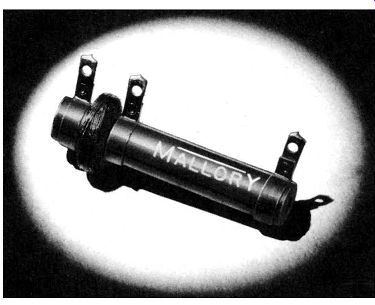
Fig. 224. Video Coupler-Combining Coupling Resistor, Shunt and Series Peaking
Coils in a Single Unit. Photo from Sample Courtesy P. R. Mallory & Co.,
Inc.
Typical Video Peaking Coils. Figures 224 and 225 show typical video peaking coils.
Figure 224 is an interesting example of a combination of the functions of the resistor and inductor in a single unit. The plate-coupling resistor (Re of Figures 221 and 222) is of the wire wound type, and is connected between the center and right hand lugs. This resistor is wound with a wire of such diameter and so spaced as to automatically provide the correct inductance for the shunt peaking element. The series peaking coil is seen at the left and is of the universal type. This provides the coupling and compensation elements of a video stage in a single unit.
Figure 225 shows two vi de o peaking coils. The coil of Figure 225A is wound on an insulated carbon resistor of the correct value to provide the required damping, while the coil of Figure 225B is wound on a bakelite form.

Fig. 225. Video Peaking Coils. Photo from Samples Courtesy F. W. Sickles Co.
PHASE SHIFT IN THE VIDEO AMPLIFIER: In our discussion of the video amplifier up to this point we have considered only the requirements of gain versus frequency. Another and equally important consideration is the possible phase shift or time-delay of the signal as it passes through the amplifier.
In the amplification of audio voltages in a broadcast receiver, phonograph amplifier or sound system, phase shift or delay of one end of the audio frequency spectrum with respect to the other is seldom of consequence. The ear is not sensitive to phase shift, and for this reason, the radio technician is not required to give it any consideration. In the case of the television video amplifier, however, phase shift and time delay are of great importance and, if not corrected, can cause badly distorted and smeared pictures.
In the reproduction of sound, wave forms are, in the great majority of cases, sinusoidal; and an understanding of the action of sine waves of voltage in passing through an amplifier is sufficient to cover the theory of operation of audio amplifiers. In television work, the video signal in many cases is of square or rectangular waveform. This c an readily be understood by considering the output obtained from the camera tube as it scans across a black bar in front of a white background. During the scanning process, the video signal is near its zero amplitude while crossing the background, and suddenly rises to maximum amplitude and remains there as the bar is crossed, dropping back to zero amplitude again as the background is reached. The length of the bar determines the half wave of a low frequency, which can be considered to be the fundamental frequency for that particular element of the picture. The square wave is composed of this fundamental frequency and a great number of harmonics of different amplitudes, which, when added up, will produce the rapid rise and rapid fall at the ends of the bar.
Thus, to reproduce a black bar, no matter what its length, will require the ability to amplify all of the harmonic frequencies which, as we have seen, can extend to four megacycles.
We have seen, in our study of the action of amplifier stages, that the wave, applied to the grid, is shifted 180° in phase when it appears across the plate load resistor.
As far as the tube itself is concerned, a wave of any frequency in the video range is shifted 180° in phase in the process of voltage amplification through a single tube. The net work of resistors and capacitors, which constitute the coupling elements between the tubes, cause a shift of phase which is different both in amount (number of degrees) and direction for different frequencies in the video range.
For the middle range (region 2 of Figure 217B) the coupling network is sensibly resistive (see Figure 218C), and a constant phase shift of 180° occurs due to the tube action.
LOW FREQUENCY PHASE SHIFT. At low frequencies (region1 of Figure 217B), the coupling network, Cc-Rg, whose effect on low frequency gain was discussed, and illustrated in Figure 217, produces a leading phase shift which increases as the frequency decreases. This phase shift is proportional to the ratio of the reactance of the coupling capacitor, to the resistance of the grid resistor, and would cause the effects shown in the table of Figure 226, if no correction were applied. It is seen that a very small phase shift, measured in degrees, can cause a large time difference at the very low frequencies.
The effect on the reproduced picture is to produce ''smearing'' of the edges of large areas and an uneven tonal reproduction of these areas. An excessive phase shift at the very low frequencies (30 to 70 cycles) will also cause a gradual shading of the picture from top to bottom, since the effect of a single picture element can exist for more than one horizontal line.
Since the phase shift is a leading effect, it can be corrected by a shunt circuit consisting of a parallel combination of capacitance and resistance of the same type of network as is required to compensate the low frequency loss of gain (R4--C4 of Figure 220). Thus both phase shift and gain can be corrected by the same network of added circuit elements.

Fig. 226. Chart Showing Low Frequency Phase Shift Due to Coupling Elements.
HIGH FREQUENCY PHASE SHIFT. At high frequencies (region 3 of Figure 217B) we find that the capacitance Ct across the coupling network can cause a lagging phase shift of the high frequencies with respect to the middle frequency portion of the video signal. Figure 227 shows the parts of the equivalent amplifier circuit (see Figure 217 and 218) responsible for high frequency phase shift. The chart shows that while the phase shift increases in degrees as the frequency increases, the time delay drops and the image displacement be comes a smaller amount. Again as in the case of low frequency phase shift, the same corrective networks which are employed to compensate for loss in gain are used to produce a phase shift in the opposite direction to that of the network. The shunt and series peaking coils and their combinations are used to produce an overall circuit phase shift which is proportional to frequency.

Fig. 227. Chart Showing High Frequency Phase Shift Due to Shunt Tube and Circuit
Capacitances.
THE IDEAL--PHASE SHIFT PROPOR TIONAL TO FREQUENCY OR UNIFORM TIME DELAY. At the speed of horizontal scanning (15,750 cycles per second), the spot moves across a picture 8 inches in width, at approximately 111,000 inches per second. This means that a time delay of one micro-second, of any part of the video signal, will produce a difference in position of almost an eighth of an inch.
If all frequencies in the video signal suffered this time delay, the picture would be satisfactory, but displaced an eighth of an inch to the right. It could be moved back by adjustment of the horizontal centering control. A uniform time delay means a different phase shift at each frequency (a phase shift proportional to the frequency).

Fig. 228. Phase Shift Requirements of a Video Amplifier for Perfect Reproduction.
The relation between time delay and frequency is expressed by the equation: Time Delay = Phase Shift in Degrees 360° Times Frequency in Cycles
Figure 228 shows the desired relationship of phase shift proportional to frequency, or uniform time delay, as applied to the video amplifier of a television receiver. It will be seen that at the high frequencies, the phase shift of the uncompensated amplifier drops below the desired proportional curve which will produce a picture without "blurred " or shifted elements.
"SMEARING" OF THE TELEVISION IMAGE BY AMPLITUDE OR PHASE DISTORTION:
Figure 229 illustrates the effects on the square wave of video modulation representing a black bar, when various deficiencies exist in the video amplifier.
Figure 229B shows the result after the square waveform has passed through an amplifier having insufficient high frequency gain.
The leading edge of the amplified wave has a gradual slope rather than an abrupt rise. This will cause shading from gray to black in the reproduction. At the trailing edge, the exponential decay of the wave will cause a gray to white smear.

Fig. 229. Square Wave Video Signals Showing the Effect of Amplifier Deficiencies.
Figure 229C shows the effect of over-compensation or excessive low frequency response. This effect is seen to be of the same nature as that caused by insufficient high frequency response, although not as pronounced.
Figure 229D illustrates the case of in sufficient low frequency response accompanied by attendant phase shift. In this case, the front edge of the bar is rendered black shading to gray, while the smear which follows the bar is white shading to gray. This type of a smear is known in television slang as a "trailer". Figure 230 shows the effect of insufficient damping of the peaking circuits used for high frequency compensation. The oscillation due to shock excitation of these circuits by the short duration square wave picture elements, can be seen as alternate white and gray ghosts adjacent to the black circular rings of the test pattern.

Fig. 230. A Station Test Pattern Showing the Effect Due to either Transient
Oscillation or a Reversed Polarity Smear. (See Figure 229C ,) Photo Courtesy
National Broadcasting Company and the R.C.A. Service Company, Inc.