INTRODUCTION
Modern digital ICs provide many of the conveniences enjoyed today. Most of these ICs require a precise power supply that controls the voltage level within narrow limits. The supply must respond very quickly to peaks and dips in current demand, because the ICs are adversely affected if certain voltage variations occur. This SECTION explains the basic methods for controlling the output of the power supply so that changes in load current and input line voltage have little or no effect on the output voltage. A power supply with its output controlled in this fashion is called a regulated power supply.
To design a regulated power supply, an unregulated supply like those described in the last SECTION is used with a regulator circuit added to its output.
This SECTION will show how a regulator can monitor the power supply output and automatically make adjustments so the output voltage stays within de fined limits. The basic functional parts of a regulator are discussed along with a variety of integrated circuits that perform these functions. These ICs simplify the design and manufacture of a regulated power supply.
WHY IS A VOLTAGE REGULATOR NEEDED?
Figure 3-1a is a schematic circuit diagram of the unregulated power supply shown in the functional diagram of Figure 2-1. Figure 3-1b shows a simplified schematic equivalent to the circuit shown in Figure 3-1a.It has a certain open circuit (no load) dc voltage as its source, V_DC, and a series resistor, R_Z, called the output impedance. Any load current, I_L flows through R_Z. Two main factors work to change the output voltage, V_o. One is a change in load current; the other is a change in input line voltage, V_IN, which changes V_dc. Sometimes these two factors occur independently, and sometimes they interact with each other.
Variations in Load Current
The dc output voltage, V_o, varies as the current demands of the load fluctuate.
Figure 3-2 plots the variations. If there is no load current (I_L =0), then V, equals V_dc, the peak ac level from the power transformer. As the load demands more current, the voltage drop across R_z causes the output voltage to fall. When the load is at the rated output current, I_RL, V_o is at V_OR, a point near the transformer's rated RMS voltage. This voltage variation is not a problem if the - load circuit demands somewhat constant current, or if the load circuit operation can tolerate the variations in V_O. For example, the power supply voltage for an audio power amplifier can vary over a considerable range without affecting the amplifier operation, as long as it doesn't dip below the level where signal clipping or other distortion occurs.
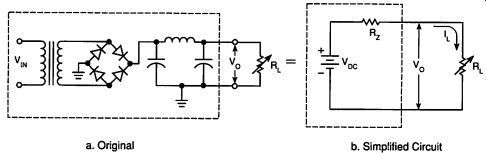
Figure 3-1. Unregulated Power Supply Circuit. a. Original b. Simplified
Circuit

Figure 3-2. Load Line of Unregulated Power Supply
Variations in Line Input Voltage
As shown in Figure 3-2, V_o also varies because the line input voltage, V_IN, varies.
If V_in changes, as it often does in many areas, the power transformer output and the filtered V_o output will change.
VOLTAGE REGULATOR PRINCIPLES
To maintain a constant V _o, a regulator circuit is inserted between Rz and R_L as shown in Figure 3-3. There is a voltage drop across the regulator, Vy; there fore, the input voltage, Vy, must be larger than V _c shown in Figure 3-1b. In Figure 3-3, Vy = Vp - (Ry + Veo).
Figure 3-3. Simplified Regulator Circuit
Regulator Action
To perform the required regulation, the regulator circuit varies V_reg; to keep V_o, constant as I, and Vic change. If I, increases, V_s increases which tends to re duce V _ however, the regulator reduces Vg to offset the increase in V, so V _ remains constant. Conversely, if I, decreases, which tends to increase V _ the regulator increases Vy; to keep V, constant. Similarly, the regulator increases or decreases V_REG if V_DC increases or decreases, respectively.
Sampling Circuit
The sampling circuit monitors the output voltage and feeds an output voltage sample to the error amplifier.
Reference Voltage Generator
The reference voltage generator maintains a constant reference voltage for the error amplifier regardless of input voltage variations.
Error Amplifier
The error amplifier compares the output voltage sample to the reference voltage and generates an error voltage if there is any difference between them.
The error amplifier output is fed to the control element to control the value of V_REG.
Control Element
The control element is essentially a variable resistance which is in series with V_DC, Rz and R_L. When V_dc or I_L changes, the input from the error amplifier adjusts this variable resistance to change V_reg to hold _o constant as explained above.
Now that the "big picture is understood," let's learn the details of the regulator circuit operation. First, the basic transistor action which is used in the circuits will be discussed.
TRANSISTOR ACTION
Transistor Construction
To clarify what is meant by transistor action, look at Figure 3-4. It is divided into three parts. Figure 3-4a shows the construction of an integrated circuit NPN transistor. The transistor is made up of islands of N, P and N semiconductor material diffused into a semiconductor wafer substrate. The most commonly used material is silicon. On the substrate, the devices next to each other are isolated from each other so they can act independently. Small gold wires are bonded to defined evaporated metal contacts to the N, P and N regions to make external electrical connections to the base (B), emitter (E) and collector (C)-the three terminals of a transistor.
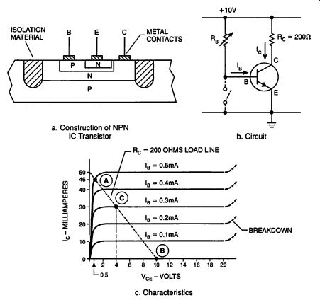
a. Construction of NPN - IC Transistor; b. Circuit; c. Characteristics
Figure 3-4. Transistor Construction and Operation
Transistor Circuit and Characteristic Curves
Figure 3-4b shows a transistor in a circuit and Figure 3-4c describes transistor action with a plot of collector current, I, against the collector-to-emitter volt age, Vi. Base current, I, flows from base to emitter when the base is more positive than the emitter by a base-to-emitter voltage, Vg, greater than 0.7V.
With a given base current, a characteristic curve of collector current can be plotted as Vis varied. Different characteristic curves are shown in Figure 3-4c for different base currents. For example, if I; equals 0.1 milliampere, then Ic is approximately 10 milliamperes for any V_s from 2 volts to 20 volts.
Notice that there is a current gain in the transistor. I. is 10 milliamperes for an I of 0.1 milliamperes; therefore, the base current controls a collector current that is 100 times greater. The current gain is not affected much by V until V _ is less than 2 volts or greater than the collector-to-emitter breakdown voltage.
Load Line
If R_c in Figure 3-4b is 200 ohms and if the supply voltage is 10V, then for any base current, I_B the V_ce of the transistor will fall on the diagonal dashed line shown on the characteristic curves of Figure 3-4c. This line is called a load line.
If I_B=0, then I_C=0 and the operating point would be at point B on the load line where V_s is 10 volts. If I_B=0.5 milliampere, then I_C=46 milliamperes, which is at point A on the load line. If I_B=0.3 milliampere, then V_s=4 volts, which is at point C on the load line. Thus, as I; varies, I; changes and V_s changes. Transistor action such as this is the basis of the regulator circuit operation in Figure 3-5.
SERIES-PASS FEEDBACK REGULATOR
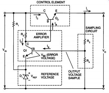
Figure 3-5. Simple Feedback Regulator
To gain more insight into the operation of a regulator, let's examine in detail the series-pass feedback regulator of Figure 3-5. The control element is NPN transistor Q2 which is connected in series between the input voltage, V_o, and the output voltage, V _in thus, the name series-pass. The load current, I_L, is the same as I_c. of Q _2 therefore, all of the load current must pass through Q2. As we learned from the discussion of transistor action, I; cannot flow unless there is an I; into Q _ thus, I_B controls I_C and I_L. How this affects the regulator operation will be discussed in a moment.
Figure 3-5 is called a feedback regulator circuit because it is a closed loop that feeds back a portion of the output voltage and compares it to a reference voltage. The difference between the two voltages determines the action that must be taken to keep the output constant.
Reference Voltage
The reference voltage, Vy, in Figure 3-5is the voltage across diode D _1 which is a special diode called a zener diode. It is operated in the reverse-biased direction, which was described in SECTION 2 as the breakdown region. Ordinary diodes would be damaged if operated in this region, but zener diodes are designed to be operated in this region.
In Figure 3-5, the input voltage to the regulator is applied to R1 in series with D1. Once the breakdown voltage of the zener diode is exceeded, the voltage across D1 remains fairly constant for wide variations of current through it. The value of R, is chosen so the required minimum current passes through D1 when V_in is at its lowest value.
Sampling Circuit
The sampling circuit in Figure 3-5 consists of two resistors, R3 and R4 in series across the output voltage terminals. The output voltage sample is the voltage across R,. This voltage depends on the ratio of the resistor values. The values of R; and R, are chosen so the voltage across R, is 0.7 volt above the reference voltage across D,. As stated previously, 0.7 volt is the Vg; voltage of a silicon transistor.
Error Amplifier
Q1 is the error amplifier and the Vbe of Q1 is the error voltage. The constant reference voltage is fed to the emitter of Q1 and the output voltage sample is fed to the base of Q1. Thus, any change in V_o varies the V_be of Q_1 which changes the base current, I_B of Q1. Changes in I_B cause the collector current, Ic of Q1 to change.
Q1 provides current gain due to transistor action. The collector current will change from 50 to 200 times the change in base current depending on the type of transistor used for Q,. R, completes the collector circuit for Q, to Vy as its supply voltage. The connection from the collector of Q, to the base of Q, provides the error-amplifier control to the control element, Q,.
Control Element
As stated previously, Q2 is a silicon NPN transistor. V_in is designed to be larger than V_o so that Q2 will always have enough V_CE for the load current range of the power supply, and still not be too large to exceed the power dissipation and temperature limits of Q,. The power dissipation in Q, at any operating point is the V_s across Q, times the current through Q,.
The emitter of Q2 is connected to the regulator output voltage terminal. The base of Q_ which is connected to Q,'s collector, is at 0.7 volt above Q,'s emitter. The base-emitter circuit of Q, is similar to the circuit of Figure 3-4b.
Base current is supplied to Q2 through R2 from the supply voltage, V_IN. I_B must be large enough to provide the maximum rated power supply load current (Ic=I_L). If Q2 has a minimum gain of 50, then the minimum base current that must be supplied through R, is the rated load current divided by 50.
Q1 controls Q2 when the collector current of Q1 shunts away (reduces) base current from Q2.
Regulator Action
Now put it all together and look at the overall regulator action. The circuit is in a stable operating condition, and then a load current decrease occurs.
A decrease in load current tends to increase V,. An increase in Vg increases the base current of Q _ which increases the collector current of Q,. The increased I. of Q, shunts away base current from Q,. The reduced base current of Q, reduces its collector current which increases its collector-to-emitter volt age. The increased voltage drop across Q, reduces Vi, An increase in load current causes opposite actions. Similar regulator control loop action occurs to keep V, constant if Vy increases or decreases. The reader should go around the loop and verify the action.
IC REGULATORS
Various combinations of the sampling element, error amplifier, and control element are available in integrated circuit form. These devices make building a regulated power supply a much simpler task than it was just a few years ago.
Three common voltage regulator ICs are presented in this SECTION.
7800-Series Fixed-Output Voltage Regulators
The LM7800-series three-terminal regulator, as shown in Figure 3-6, is a series-pass regulator which has a V _ terminal, a Vy; terminal, and a ground terminal. Rated output voltages from 5 to 24 volts are available in the 7800 series. The last two digits of the part number indicate the output voltage of the regulator. For example, the 7805 is a 5-volt regulator, the 7812 is a 12-volt regulator, and the 7815 is a 15-volt regulator. The regulated output voltage is fixed for each regulator.
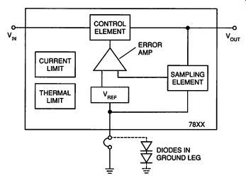
Figure 3-6. 7800-Series Regulator
The regulator contains all of the functions shown in Figure 3-3. In addition, it contains protection circuits to limit the peak output current to a safe value, and to maintain the internal power dissipation to a safe limit. A thermal shutdown circuit operates if the internal power dissipation exceeds a preset value. With proper heat sinks, the 7800-series can supply 1.5 amperes of load current. Notice that in order for the output voltage to be at the rated value, the sampling element must have a good ground point close to the load.
As shown in Figure 3-6, the output of the regulator can be increased by raising the regulator ground to a voltage above ground. The dotted lines show two 1N4001 diodes connected in series with the regulator's ground pin. Due to the forward-bias voltage drop of the silicon diodes, the ground pin of the regulator will be 1.3 to 1.4 volts above the ground level, causing the output to be 1.3 to 1.4 volts above the rated fixed-voltage output. Regulation suffers slightly because only a portion of V, is being sampled. Higher offsets can be obtained by using more diodes, or by using a reverse-biased, high-current zener diode. Such techniques are useful to increase the fixed output voltage by a volt or two.
LM317 Adjustable Voltage Regulator
The LM317 three-terminal adjustable voltage regulator is similar to the 7800 regulator, except that it doesn't have an internal sampling element, and the ground terminal is replaced by an adjustment (AD]) terminal. This terminal is connected to an external voltage divider which serves three purposes. The first is to provide a sampling-element voltage to the built-in error amplifier. The second is to provide enough current from ground through R1 to operate the circuit's built-in voltage reference. The third is that it makes it easy to design an adjustable power supply. The built-in control element, an NPN transistor, is large enough to allow the LM317T to supply 1.5 amps if adequate heat-sink surface is used. The LM317T has built-in protection for maximum current and for exceeding internal power dissipation over its rated temperature range.
The operation of the LM317 is somewhat different from the 7800 series because it is what's known as a "floating regulator." It maintains its reference voltage relative to the output voltage, V _; therefore, whenever it operates, it adjusts its operating point so that the voltage across R, in the R _ R, voltage divider is always equal to its reference voltage, Vy. As a result, as shown in Figure 3-7,V, is equal to Vig (1.25V in the case of the LM317) times one plus the ratio of R, to R,.IfR, is 9 times R _ then for an LM317, Vis 10 times 1.25V, or 12.5 volts.
One can easily see that if R, is an adjustable resistor, V _ can be adjusted over a wide voltage range, provided V,y is within the proper range. The minimum Vix must be greater than Vg + Vig. The maximum V, cannot be greater than V _ + 40 volts; for example, if V,=12 volts, V _ cannot be greater than 52 volts. Of course, the greater Vp, the greater the internal thermal dissipation.
Remote Sense
Another advantage of the external sampling element is that remote sensing is made easy. In many system designs, long power distribution leads cannot be avoided. A long power supply lead that has a high current will have a significant voltage drop which is outside the regulation loop. To solve the problem, remote sensing is used. A separate wire is connected to the actual load point and feeds back the load voltage directly to the sampling circuit. Because there is very small current in the wire, the voltage drop is negligible, and the regulation at the load point is much improved.
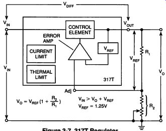
Figure 3-7. 317T Regulator
723 Regulator IC
The 723 regulator is shown in Figure 3-8. It contains a reference voltage source, an error amplifier, a low-current control element, and two extra components-a zener diode and a transistor. The extra transistor is used as a current limiter. As illustrated, using the 723 requires more external components to build a power supply than the 7800 and 317 regulators; however, because the basic functions are available at the external pins, the 723 is a very versatile regulator. Low-current (150 mA) stand-alone supplies use the 723, but its most common use is to drive a much larger current-handling control element.
Adding External Transistor For Higher Output Current
Figure 3-8 shows how an external transistor that can handle much larger current is connected to the 723 to provide a higher-current control element.
The collector of the external transistor is connected to V, of the 723. The base is connected to Vy, and the emitter becomes the new Vg; terminal for the larger-current regulator. The 723 becomes a driver for the external control element. A proper heat sink must be used to keep the external transistor in the safe operating area.
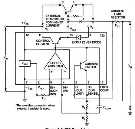
Figure 3-8. 723 Regulator
REGULATOR PROTECTION
A power supply regulator handles a considerable amount of energy while doing its job. If the electrical and thermal forces get out of control, the circuit can destroy itself. Manufacturers of IC regulators, and other IC semiconductor devices that may be added externally, specify maximum voltage, current, and temperature limits that must not be exceeded. When a circuit design stays within these limits, all components are in their safe operating area. Operation beyond these limits may destroy the device. To assure that regulators will not be destroyed if limits are exceeded, protection circuits are added to the regulators.
Short-Circuit Protection
A common occurrence is that a regulator's output terminal is shorted to ground. When this happens, the regulator tries to supply a large current beyond its rated value. As previously discussed, short-circuit protection circuits are built into 7800-series and LM317T regulators. For the 723, as shown in Figure 3-8, the current limiter transistor is connected to measure the voltage drop across a low resistance in series with the output terminal. As the load current increases, the voltage drop across this resistance increases. If this voltage rises above the Vi; of the transistor, it indicates excessive current demand by the load. The current limiter transistor conducts and shunts base current from the control element to limit its I, which is the load current. This keeps the control element in its safe operating area.
Thermal Runaway
Excessively high temperatures cause real problems in the operation of IC regulators or any other solid-state circuit. If the maximum junction tempera ture specified on a device's data sheet is exceeded, the device is usually destroyed. Junction temperature rises because of power dissipation. The expected power dissipation generated by a series-pass regulator is calculated by multiplying the voltage drop across the control element (Vy -Vg) by the current flowing through it. This power is converted to heat which raises the junction temperature. If this heat is not removed more quickly than it builds up, a condition called thermal runaway can occur. The heat causes the device to conduct more current, resulting in more heat, until the device literally destroys itself. As long as the limits for the particular device are not exceeded, the device will remain in its safe thermal operating area.
Thermal Conduction
To protect semiconductor junctions from excessive temperatures, a path must be provided to conduct the heat away from the silicon substrate where it is generated. The usual path that the heat must travel is from the silicon to the IC package or case to the surrounding air. If the device is operated well below its maximum ratings, this usually is an adequate conduction path; however, as the power increases, the heat must be removed more rapidly.
Heat Sink
A heat sink is a piece of metal attached to a semiconductor device case oran IC package for the purpose of conducting heat away from the device. The larger the surface area of the heat sink, the faster heat is removed by conduction and radiation into the surrounding air. Figure 3-9shows how the metal, which is a much more efficient thermal conductor, keeps the IC from becoming too hot.
Heat flows from the silicon chip, to the IC package, then to the air through the leads, printed circuit board, and heat sink.

Figure 3-9. Heat Flow From IC to Heat Sink
To increase the efficiency of the heat transfer from the package to the heat sink, a thermally conductive compound is often used between them. If it is necessary to electrically insulate the device from the heat sink, a mica insulator is used. Radio Shack's power semiconductor mounting kit, 276-1371, includes such an insulator.
Sometimes the conduction and radiation cooling of the heat sink is not enough to keep the power device below its maximum junction temperature. In this situation, a fan is used to move air across the heat sink to increase convection cooling. In any design, temperature measurements should be made to ensure that maximum temperatures are not being exceeded.
SUMMARY
What has been learned? -- how an available ac line voltage can be transformed to a level close to the dc voltage needed, how rectification and filtration can give a steady dc voltage, and how a regulator provides a precise voltage even under varying input voltage variations and output current demands. In SECTION 4, these principles will be put to work in useful projects.
Prev: SECTION 2 UNREGULATED POWER SUPPLY SYSTEMS
Next: SECTION 4 LINEAR POWER SUPPLY PROJECTS
Building Power Supplies (Article Index)
Also see:
Link |