This SECTION contains three power supply projects using the principles developed in the previous three SECTIONs. These projects use commonly available parts from Radio Shack.
REGULATED 5-VOLT POWER SUPPLY
The first project is a regulated +5V power supply that can be used to power digital circuits. This is an ideal power supply for experimentation using IC breadboards such as Radio Shack's No. 276-169.
Requirements
Digital integrated circuits are available for nearly any purpose in a wide range of complexities. As varied as they are, the vast majority require a supply voltage of 5 volts regulated to within 10%; however, some of the more complex ICs, such as microprocessors, require 5% regulation.
Regulation
The percentage of load regulation is expressed as follows:
%Load Reg = (Vy, - V/V, X 100
It is the change in voltage, expressed as a percentage, that occurs when the load changes from no-load (NL) to a load (L) divided by the load voltage. It is a measure of how far the output voltage varies in response to rapid changes in current demand by the load. Let's verify the output voltage of a 5V supply with a regulation of 5% using the load regulation equation. In the following calculation, V, is the Vy, - V, variation in the above equation.
+5% = V,/5 X 100
+0.05 = V,/5
+V, = 5(+0.05) = +0.25
-V, = 5(-0.05) = -0.25
Therefore, with +5% regulation, the 5V output voltage will vary from 5.25 to 4.75 volts regardless of the rapid peaks and dips in current demand. This regulation also applies to input voltage changes.
Load Current
The current demands of digital ICs vary from a few milliamps for logic devices to a few hundred milliamps for complex ICs. Power switching devices often control load currents of 100 mA or more which drive motors, contactors, lamps or relays. This current is in addition to the current for the logics internal circuitry. As a result, a +5V supply with a maximum rated current of 1A (1000 mA) and a possible current of 1.5A (1500mA) should be sufficient to handle small projects and experiments that consist of around 10 ICs and some power devices.
Ripple
The ripple specification is derived using the input capacitor filter equation (from SECTION 2) and the fact that the regulator compensates for ripple voltage variations at its input. This regulator characteristic is called ripple rejection.
Digital logic circuits usually have a minimum of 200 millivolts noise mar gin around critical logic levels in their system design. Any power supply ripple reduces the amount of "headroom" (tolerance) on this design margin. Thus, if ripple voltage were to cause logic levels to vary by 20 millivolts, it would reduce the noise margin by 10%.
An input capacitor filter, CF _ with a capacitance of 4700uF is chosen for this project. At a 1500mA load, the ripple voltage is:
Vins = 2-4 X 1500/4700 Vins) = 0.76 or 760 millivolts
The 7805 regulator will be used in the design. It has a ripple rejection characteristic of 60 decibels. The decibel, which is abbreviated dB, is the unit used to express the ripple voltage that appears at the output of the regulator when a certain voltage appears at the input. The relationship (a reduction) is expressed as follows:
-60dB = 20log _ Vo/ Vin -3 = log, Vo/ Vin 10^-3 = V/V
It means that the output ripple voltage, V _ will be reduced by 1000 times over what appears at the input, Vy. Since the input ripple voltage is 760 milli volts, it should be 0.76 millivolts at the regulator output. This is small enough to cause no problem with noise margin.
The schematic diagram for the full supply is shown in Figure 4-1.
Protections
Here are a number of protections built into the design.
1. The power switch, S1, is a double-pole double-throw (DPDT) switch with the line cord connected to one of the outside pairs of terminals. This isolates the line voltage inside the switch body when the switch is off.
2. An input fuse is in series with one of the primary leads of the transformer to protect against transformer shorts.
3. An LED indicator is wired across the output terminals as a pilot light and an aid in determining when the filter capacitors have discharged.
4. A fuse in series with the output helps prevent an experiment from "going up in smoke." It has been included to demonstrate its use in a design. It really ...
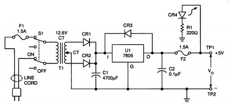
Figure 4-1. Regulated +5V Power Supply Schematic
...isn't necessary because the 7805 regulator has current limiting. If the regulator used has no short-circuit protection, the fuse is absolutely necessary for experimental supplies like this.
5. Since this supply may be used with a variety of loads, a diode is connected from the input to the output so that it is reverse biased under normal operation. This provides protection if a large amount of capacitance is connected to the output. When the input voltage is turned off, the large capacitance on the output may discharge more slowly than the capacitance on the input. This would reverse bias the regulator and could damage it. The diode provides a "safe path" for the discharging current.
Regulator Choice
The requirements for this regulated +5V power supply project closely match the ratings of the fixed-voltage 7805 IC regulator->5 volts output voltage and 1.5 amperes maximum load current. The built-in thermal cutoff circuit and current limiting features are especially useful to provide additional protection when powering your experiments.
Since the 7805 IC will be delivering a power supply rated current of 1 ampere and a possible maximum current of 1.5 amperes, and since its minimum standoff voltage is 3 volts, it will dissipate a minimum of 4.5 watts at maximum load. It must be and is mounted in a heat sink and cooling holes are drilled in the enclosure to prevent heat build up.
Transformer and Rectifier
Choice The 7805 IC regulator requires a minimum voltage differential between the input and output of 3 volts. Thus, to obtain a 5-volt output, the input to the regulator must be at least 8 volts. The transformer's center-tapped secondary is rated at 12.6 volts at 3 amps. Using the two-diode full-wave rectification scheme produces 8.9 volts peak (6.3 X 1.414) at 3 amps. The rectifier diodes, which require a PIV of 17.8 volts, and the protection diode across the regulator are rated at 3A, 50V PIV. By choosing an 18V center-tapped transformer (RS# 273-1515), the supply would be able to operate at 1.5A continuously because the peak voltage is raised. However, the heat sinking of the 7805 regulator has to be more extensive to protect the regulator from exceeding the power dissipation and case temperature limits.
Filters The filtering and resultant ripple voltage is as previously described for the 7805 regulator. A small capacitor (0.1uF) is placed across the output of the regulator to bypass high-frequency noise that may be generated by the load.
Construction Details
The parts listed in Table 4-1 are used for this project.
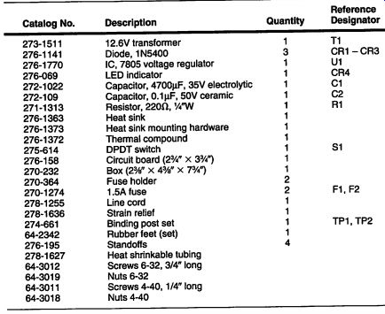
Table 4-1. Regulated +5V Power Supply Parts List
Construct the circuit on the circuit board following the connection dia gram in Figure 4-2 and the photograph in Figure 4-4. Figure 4-2 shows the underside of the circuit board. Insert the component leads through the board in the positions shown, and bend the leads as shown against the bottom of the board to hold the components in place. Besides the leads, extra lengths of bare or insulated wire are used to make the connections.
Use thermal compound between the IC and the heat sink when mounting he regulator IC. Use a 6-32 screw and nut to hold the IC in place. Insert the regulator pins through the holes in the board, wrap the component leads and wire connections around the pins, and then quickly solder the connections without heating the IC excessively. Remember, shiny solder connections are proper connections, not grainy gray. The solder on the IC leads should wet the contacts on the board to hold the IC in place, but make sure the leads do not short together.
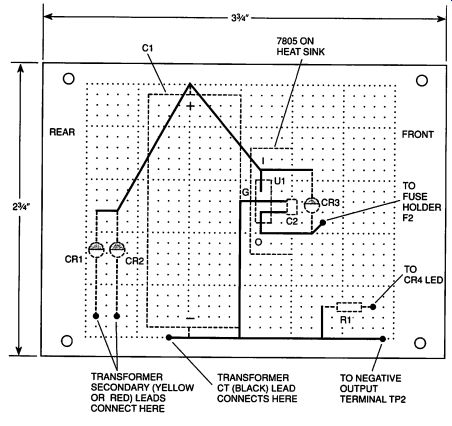
Figure 4-2. Regulated +5V P.S. Circuit Board Parts Placement (Underside
shown)
TRANSFORMER TO NEGATIVE SECONDARY ( YELLOW CT (BLACK) LEAD OUTPUT OR RED) LEADS CONNECTS HERE TERMINAL TP2 ; CONNECT HERE
Enclosure-Mounted Components
Remove the bottom cover from the box. Refer to Figure 4-1 a for a pictorial view.
Drill mounting and cooling holes in the box in the positions shown in Figure 4-3. The 1/8" holes are for mounting the circuit board and the transformer. The front panel holes are for fuses, binding posts, an indicator, and a power switch.
The 3/8" end hole is for the line cord.
While the circuit board is unmounted, insert the two secondary (red or yellow) transformer leads through the board, and solder each to a formed diode lead on the underside of the board. Do the same with the centertap (black) lead, but solder it to the negative lead of capacitor C1. Insert a red wire through the board at the junction of CR3, C2, and the output pin of the 7805 and solder it in place. This is the positive output voltage lead to F2. Insert a black wire through the board at the negative lead of C1 and solder it in place.
This is the negative output voltage lead to terminal TP2. Insert another black wire through the board and connect it to R1. This wire will be connected to the LED. Mount the standoffs to the circuit board with the short 4-40 screws.
Assembly Steps
1. Mount the transformer upside down directly to the box top in the position shown in Figure 4-3. Use 6-32 screws and nuts.
2. Install the fuse holders, binding posts, LED, and power switch in the front panel as shown in Figures 4-3 and 4-4. Mounting hardware is on the components.
3. Mount the circuit board on standoffs inside the box in the position shown in Figure 4-3. Use the short 4-40 screws.
4. Insert the ac line cord through the strain relief and anchor the strain relief in the end 3/8" hole. Allow 2" of slack inside the box.
5. Solder the primary leads of the transformer to the center pair of terminals on the power switch. The switch handle up indicates the power supply is on and that the bottom terminals are internally connected to the center terminals.
6. Solder one wire of the ac line cord to the side contact on the fuse holder for F1.
Run a wire from the end contact of the fuse holder to one terminal of the bottom pair of terminals on the power switch. Solder the other wire of the ac line cord to the other bottom switch terminal. Insert a 1.5A fuse in the holder.
7. Solder the negative black wire from the circuit board to the lug from the black binding post TP2, then secure the lug to the post with the nut provided. This is the negative terminal of the output voltage.
8. Solder the positive red wire from the circuit board to the end terminal of the fuse holder for F2. Insert a 1.5A fuse in the holder.
9. Solder a red wire from the side terminal of the fuse holder, F2, to the red binding post (TP1) lug. Secure the lug to the post with the nut provided. This is the positive terminal of the output voltage.
10. Solder the black wire from R1 to the short lead of the LED.
11. Slip a small piece of heat-shrinkable tubing over a red wire and solder it from the long lead of the LED to the lug on TP1. Pull the tubing up over the LED connection.
12. Recheck all connections against the schematic in Figure 4-1. Correct any errors.
13. Attach the cover with the self-tapping screws provided. Mark the position for the rubber feet, strip off the self-adhesive covering, and stick the feet in place.
14. Connect a voltmeter to the output, plug in the ac cord, and flip the power switch on to test the output voltage before using the supply. The open-circuit output voltage should be 5 volts and it should not change more than 5% when a resistive load drawing rated load of 1 amp (5 ohms) is placed across it.
a. Drilling Pattern for Top
b. Drilling Pattern for Front Panel
c. Drilling Pattern for Rear Panel Figure 4-3. Chassis Layout for +5V Power Supply
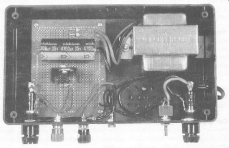
Fig. 4-4
REGULATED +12V POWER SUPPLY
This project is a dual power supply with a +12V output and a -12V output around a common ground.
Requirements Output Voltage
Many analog ICs and some digital data communication ICs operate on differential power supplies. Such power supplies usually have a central ground with equal positive and negative voltage outputs. There are specialized ICs that require different positive and negative voltages; if this is a requirement, the design principles for setting the voltages are the same.
Load Current
Many analog applications are for small-signal amplification. As a result, the load currents are quite small; therefore, a rated load current of 1.5 amperes for each differential voltage should be quite adequate for many systems. Even if the application is a power amplifier that delivers 10 to 12 watts, the design should be adequate.
Ripple
Small-signal analog circuits require even lower ripple voltages than logic circuits; therefore, the regulator chosen for this design must have an even higher ripple rejection characteristic than the +5V supply. If the supply needs further ripple reduction, more filter sections can be added to the input filtering, or, as will be mentioned for the LM317 regulator, additional components can be added to the regulator circuit.
Regulation
It is not likely that the current changes due to signals are going to be as severe in analog circuits as in digital circuits; however, much smaller voltage changes become significant signals in the analog circuits. For this reason, the regulation of the differential supply voltages is set at 0.5%, with a maximum of 1% over wide temperature swings.
Protection
Similar protection features to those included in the +5V supply are included in this design-a primary fuse, a DPDT power switch, and an LED pilot light.
Component Choices
Because negative regulator ICs are not as widely available as positive regulator ICs, this project uses two LM317T adjustable regulators and separate 25.2-volt center-tapped transformers for each side.
The schematic diagram in Figure 4-5 shows two independent power sup ply circuits connected in series at their output, with the ac input in parallel.
This is possible because of the isolation provided by the power transformers.
The positive lead of the second supply is connected to the negative lead of the first, forming the central ground. The specifications of the supply are:
Output voltage: +/- 12V, 0.5% typical, common central ground.
Output current: a maximum of 1.5 amps for each voltage.
Ripple: 65 to 80 dB typical rejection.
The peak voltage output across the capacitor input filter is 17.8 volts (12.6 X 1.414). Two 1N5400 diodes are used for full-wave rectification, with the center taps of the transformers used as the negative terminals. The diodes are rated at 3 amps, 50 PIV, well within the 35.6V PIV required.
The LM317T regulator offers the added advantage that the output voltage can be changed simply by changing the ratio of the resistance between the adjustment pin and ground and the resistance between the adjustment pin and the output. For 12 volts output, using 390-ohm resistors for R1 and R3, the programming resistors R2 and R4 are calculated by using the equation:
Vo = 1.25[1+(R2/R1)] Vo/1.25 - 1 = R,/R,
Substituting 12V for V _ gives:
12/1.25 -1 = R,/R, 9.6 -1 = R,/R, 8.6R, =R, IfR, = R,= 390-ohm, then R, = R, = 33000.
Figure 4-5. Regulated + 12V Power Supply Schematic
The LM317 has a typical ripple rejection characteristic of 65dB. It can be raised to 80dB by bypassing R, and R, with a 10pF capacitor (shown as C5 and C6). Since the same capacitive input filter is used as in the +5V supply, the input ripple will be the same-760 millivolts. With 65dB rejection, the output ripple is over 2000 times less. At 80dB rejection, the ripple at the output is reduced by 10,000 times.
Construction Details
The parts listed in Table 4-2 are used for this project.
Construct the circuit on the perfboard following the connection diagram in Figure 4-6. Scribe the perfboard along a row of holes to obtain the 3" X 6" dimensions, then snap the board along the scribe line. As in the other projects, insert the leads of the components through the board in the position shown, bend the leads over against the bottom of the board, and make the connection to the underside of the board as shown in Figure 4-6. Add extra wire to complete all connections, and solder component leads and wire together.
Insert through the board, at the positions shown in Figure 4-6, two red wires, one black wire, and two wires of another color. Solder one red wire to the negative output, TP3, and the other red wire to the positive output, TP1. Solder ...
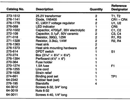
Table 4-2. Regulated + 12V Power Supply Parts List
... the black wire to the ground connection, TP2. The other colored wires will connect to CR5. Solder one to the junction of CR1 and CR2, and the other to the end of R5. Mount the standoffs at each corner of the board with short 4-40 screws.
Enclosure-Mounted Components
Drill mounting and cooling holes in the bottom and top of the enclosure as shown in Figure 4-7. Refer to Figure 4-14bfor a pictorial view. The transformer and perfboard mount to the inside of the bottom. Install the rubber feet to the bottom with the self-adhesive pads in the position indicated in Figure 4-7.
Assembly Steps
1. Install the binding posts and LED to the front panel portion of the bottom, and the power switch and fuse holder to the rear panel as shown in Figures 4-7 and 4-8.
2. Insert the ac line cord through the strain relief and anchor the strain relief in the 3/8" hole in the rear panel. Allow 2" of slack inside the bottom.
3. Mount the transformers to the bottom near the rear panel as shown in Figure 4-7.
Use 6-32 screws and nuts.
4. Solder one wire of the ac line cord to the end contact on the fuse holder or F1. Run a wire from the fuse holder's side contact to one terminal of the bottom pair of terminals on the power switch, S1. Solder the other ac line cord wire to the other bottom switch terminal. Solder the primary leads of the transformers to the center pair of terminals. Insert a 1.5A fuse in the fuse holder. When the switch handle is up, the power supply is on.
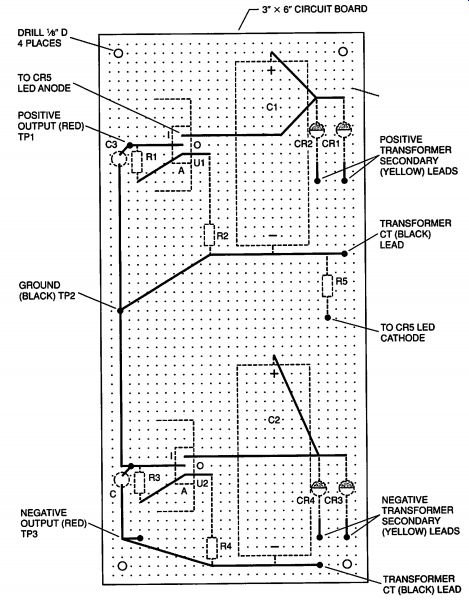
Figure 4-6. Regulated +12V P.S. Circuit Board Parts Placement (Underside
Shown)
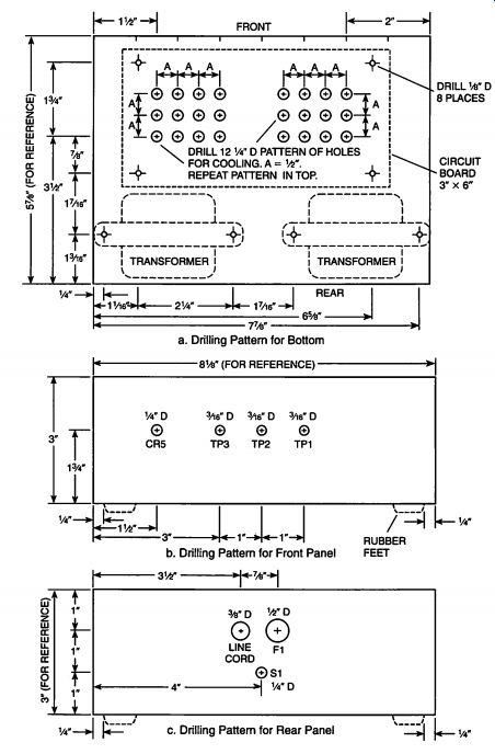
Figure 4-7. Chassis Layout for +12V Power Supply
a. Drilling Pattern for Bottom
b. Drilling Pattern for Front Panel
c. Drilling Pattern for Rear Panel
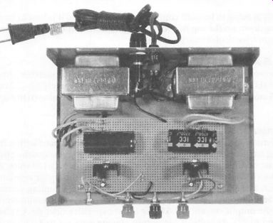
Figure 4-8. Fully Assembled + 12V Power Supply
5. While the perfboard is unmounted, insert the two secondary (yellow) leads of each transformer through the board and solder each to a formed rectifier diode lead on the underside of the board. Follow the diagram carefully. The negative transformer leads go to CR3 and CR4; the positive transformer leads to CR1 and CR2. Insert the black centertap transformer leads through the board. The negative transformer black lead is soldered to the negative output connection; the positive transformer black lead is soldered to ground. Mount the standoffs to the board with short 4-40 screws.
6. Mount the perfboard with its standoffs to the bottom of the box with short 4-40 screws into the standoffs.
7. Solder the red negative-output lead from the circuit board to the lug from the red negative-output binding post (TP3), then secure the lug to the post with the nut.
8. Solder the red positive-output lead from the circuit board to the lug from the red positive-output binding post (TP1), then secure the lug to the post with the nut.
9. Solder the black ground lead from the circuit board to the lug from the black ground binding post (TP2), then secure the lug to the post with the nut.
10. Slip a small piece of heat-shrinkable tubing over the wire from R5 and solder it to the short lead on CR5. Do the same for the remaining wire from the board, but solder it to the long lead on CR5. The LED indicator is now connected. Slip the tubing over the connections to CR5.
11. Recheck all connections against the schematic in Figure 4-5. Correct any errors.
12. If cooling holes have not been drilled in the top, do that now.
13. Connect a voltmeter to the output, plug in the ac cord, and flip the power switch on to test the output voltages before using the supply. Each output voltage should be 12 volts and remain within 1.0% regulation when a load from milliamperes to 1.5 ampere is placed across the supply (an 8(2, 20W power resistor must be used for 1.5A).
CAUTION If the supply is going to be used continuously at 1.5A, then it is best to have a fan blowing down on the top to keep the regulator within its limits of power dissipation at a particular case temperature.
VARIABLE POWER SUPPLY
The last project for this SECTION is a power supply with a variable output voltage suitable for a wide range of uses. It covers approximately 3.0 - 30 volts at up to 1.5 amps of current in three ranges. The schematic is shown in Figure 4-9.
Transformer and Regulator
The transformer is a 25.2V, 2A, center-tapped transformer used with a full wave bridge rectifier rated at 1.5A, 50VPIV, to provide 35.6 V _ (minus the bridge diode drops), or a few volts higher if the ac line voltage is over 120 volts. The regulator is an LM317. Since the LM317 regulator is used, the typical regulation specification is 0.5% just like the previous supply. The sampling element includes a variable resistor (5K) to provide a front-panel voltage adjustment.
When the output current is 1.5A, the input capacitive filter peak voltage has dropped to 27 - 28 volts. If the output voltage were set to 3.0 volts, the regulator would have to drop over 25 volts. Thus, at 1.5 amps, the regulator would dissipate over 37.5 watts as heat, which would quickly trigger the device's thermal-shutdown protection circuit.
To keep the power dissipation of the regulator within acceptable values, the operating range of the supply is divided into three ranges. Within each range, switching is designed to limit the minimum output voltage, and the input voltage to the regulator at maximum current. A voltage dropping resistor is placed in series with the regulator to control the input voltage, while the minimum voltage for each range is set by the resistor ratio in the sampling element. For example, for the low range, R1 plus R2 is 740 ohms and R6 plus R7 is a minimum of 740 ohms. The ratio of R6 plus R7 to R1 plus R2 is 1. Using the equation:
Vo = 1.25(1 + (R6+R7)/(R1+R2))
.... the minimum voltage for the range is 2.5 volts (1.25(1+1)). The minimum differential voltage across the LM317 is specified to be 3 volts; however, many of the regulators will operate down to 2.5 volts. By inserting a 9 ohm resistor in series right after the capacitive input filter, the input voltage to the regulator is limited to 14.5 volts when the load current is 1.5 amperes. The resistor not only serves as a series dropping resistor, but also as the resistive part of another resistive-capacitive filter section formed with C2.
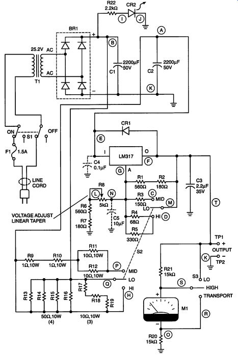
Figure 4-9. Regulated Adjustable Power Supply Schematic
The approximate voltage drops across the series resistance for the low and mid ranges is as follows:
Range Rg 1.0A 1.5A LO 9Q gv 13.5V MID 4Q 4V 6V Ripple
As in the previous supply using the LM317, the ripple rejection is either 65dB, or, if bypass capacitor C5 is used, it increases to 80dB. Using the ripple voltage equation, the ripple voltage input to the regulator is calculated as:
Vrl(rms) = 2.4 X 1500/2200 = 1.64 volts
With 65dB of ripple rejection, the ripple voltage at the regulator output is reduced over 2000 times to below 0.82 millivolts. Actual measurements show this to be from 3 to 10 millivolts. Long leads due to the switching seem to contribute to larger ripple.
The output capacitor C3 is a 2.2 uF tantalum capacitor whose main task is to prevent noise generated by the load from affecting the regulator operation.
If a layout of a power supply design were to place the filter capacitors a fair distance from the regulator, then the 0.1uF capacitor C4 (indicated in dotted lines) would be added to the design.
Indicators A LED pilot light and a meter are used to indicate voltage presence. The LED, with a current-limiting resistor (2.2 k-O), indicates the presence of dc (prior to regulation). The meter indicates the output voltage and a range switch changes the full scale from 15 volts to 30 volts. The TRANSPORT position of the switch, which shorts across the meter, should be used when the supply is being moved.
Heat Sinks
Because of the high power dissipation in this supply at the current extremes, the regulator and TO-220 heat sink are mounted to the back of the enclosure.
The regulator is insulated from the heat sink. This provides maximum heat sink area for thermal protection. However, if the supply is operated continuously at voltage and current conditions near the maximum boundaries indicated in Figure 4-10, a fan should be directed to blow over the back of the enclosure as an added precaution to protect the regulator.
Figure 4-10. Operating Regions for Adjustable Power Supply
Operating Region As shown in Figure 4-10, there are regions within the operating voltage ranges where the maximum power dissipation of the LM317 (15W @ T;=25-90°C) is being exceeded. The power supply should not be operated within these regions.
Other operating restrictions also are shown:
1.The peak voltage output from the transformer and rectifier at various currents and the 3V minimum differential across the LM317 limit the maximum output voltage to 25 volts at 1.5A.
2.The maximum load current for the LM317 is 1.5A.
3.The three nominal voltage ranges are:
LO: 3.0to 11 volts MID: 9.5 to 20 volts HI: 18.0 to 30 volts
The voltage adjustment varies with the ranges. A full turn of the knob is required on the LO range, approximately half of the sweep is required on the MID range, and less than half of the sweep is required for the HI range. As the output voltage on each range is increased, the differential voltage across the LM317 decreases, and (especially at high currents) may drop below 3 volts.
This causes the LM317 to drop out of regulation.
Construction Details
The parts listed in Table 4-3 are used for this project:
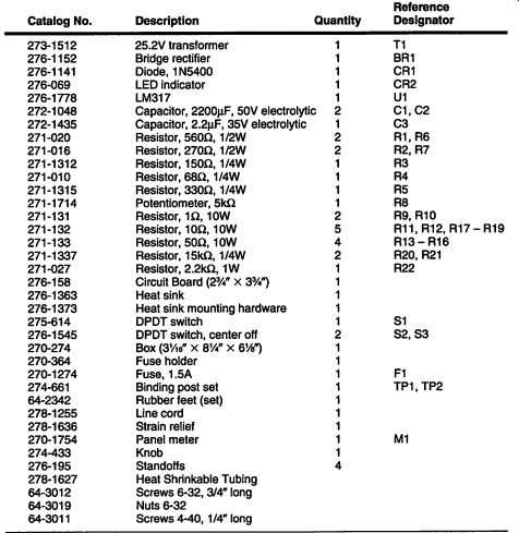
Table 4-3. Variable Power Supply Parts List
Circuit Board
As with the previous projects, insert the components through the circuit board in the positions shown in Figure 4-11, bend the leads, and interconnect the circuit. Use extra wire as necessary. Insert three 2" wires through the board at points E, F, and G, respectively, as shown, and solder in place. Remember Figure 4-11 is the underside of the board. Slip short lengths of shrinkable tubing over the wires. These wires connect to the LM317, which is mounted on the rear panel of the enclosure.
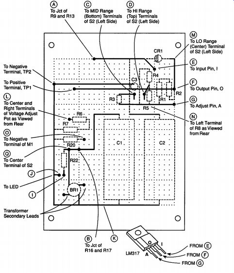
Figure 4-11. Adjustable P.S. Circuit Board Parts Placement (Underside Shown)
Insert 7" lengths of wire for A, C, D, 1, J, L, M, N and O, and two lengths at B, and solder in place. Make these wires different colors so they can be identified easily. A will be in the main output supply line to the LM317 and connects to C2. B is the V _ voltage line to the series dropping resistors and to the range switch, S2, controlling the voltage ranges. The connection to S2 is called Q. C, D, and M connect to one side of the range switch, $2; I and J connect to CR2; L and N connect to the adjustment control, R8; and O connects to M1 for full scale of 15 volts.
Insert a 6" red and black wire through the board at TP1 and TP2, and solder in place. TP1 will connect to the positive output voltage terminal and TP2 to the negative output voltage terminal.
Drill holes in the enclosure as shown in Figure 4-12. Refer to Figure 4-14b for a pictorial view of the enclosure. Install the rubber feet to the bottom with the self-adhesive pads.
Assembly Steps
1. Proceed carefully one step at a time. The interconnections are a bit complicated.
Refer to Figures 4-9, 4-11, 4-12, and 4-13 at each step.
2. Install the power switch, fuse holder, and ac line cord in strain relief in the rear panel. Leave about 2" line cord slack inside the box. y
3. Solder one wire of the line cord to the end contact on the fuse holder for F1. Run a wire from the fuse holder's side contact to one bottom terminal of the power switch, S1. Solder the other line cord wire to the other bottom switch terminal. Insert a 2A fuse in the fuse holder.
4. Mount the transformer to the bottom of the enclosure. Solder the primary leads to the center pair of terminals of S1. When the switch handle is up, the power supply is on.
5. The power resistors are stacked and held in contact with the enclosure bottom by two wire ties, as shown in Figures 4-12 and 4-13. Pass the ties through the holes in the bottom of the enclosure to hold the resistors in place. Interconnect and solder the leads of R9 through R18 shown in Figure 4-9. Attach two wires to form the connection H and the connection P from the resistors to the range switch, S2.
6. Install the front-panel components, S2, S3, CR2, TP1, TP2, R8 and M1.
7. Mount the regulator IC on the heat sink with the insulator provided in 276-1373 between the IC and the heat sink. With the same screw and nut, attach the heat sink to the rear of the enclosure. Use thermal compound on all surfaces.
8. Before mounting the circuit board, insert the transformer secondary leads through the circuit board as indicated in Figure 4-11, and solder in place.
9. Mount the circuit board to the standoffs, and mount the assembly to the bottom in the position shown in Figures 4-12 and 4-13. Use 4-40 screws.
10. Solder wires E, F, and G to the LM317 as shown in Figure 4-11. Trim wires to length and slip shrinkable tubes over connections.
11. Looking at the voltage adjustment resistor, R8, from the rear, solder N to the left hand terminal. Solder L to the center terminal and right hand terminal, shorting the terminals together.
12. Slip a small length of heat shrinkable tubing over the LED wires, | and J, and solder them to the LED indicator leads. J connects to the short lead (cathode); | connects to the long lead (anode). Slip tubing over connections.
13. Solder the positive red wire to the lug of TP1, and the negative black wire to the lug of TP2. These are the output voltage binding posts.
14. Solder wire O to the negative terminal of the meter, M1. Solder a wire, R, from the negative terminal of M1 to the bottom right-side terminal (looking from rear) of S3.
15. Run a wire S from the positive terminal of M1 to the center right-side terminal of S3. Also, between this same terminal and the top terminal of S3, connect R21. R21 makes M1 into a 30V full-scale meter. Complete the M1 connections by running wire T from the top terminal of S3 to the lug of TP1. Solder all connections.
16. Solder wire A to the junction of power resistors R9 and R13. At this junction is wire H from step 4. Solder H to the top right-side (looking from rear) terminal of S2.
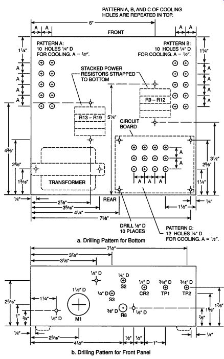
Figure 4-12. Chassis Layout for Adjustable Power Supply
a. Drilling Pattern for Bottom
b. Drilling Pattern for Front Panel
c. Drilling Pattern for Rear Panel
Figure 4-12. Chassis Layout for Adjustable Power Supply (Continued)
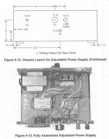
Figure 4-13. Fully Assembled Adjustable Power Supply
17. Solder wire Q to the center right-side terminal of S2, and wire P to the bottom right side terminal. When the handle of S2 is up, S2 is on MID range; when it is down, it is on the HI range; and when it is in the center, it is on the LO range.
18. Solder wire C to the bottom left-side (looking from rear) terminal of S2, wire M to the center terminal, and wire D to the top terminal.
19. Recheck all connections against the schematic in Figure 4-9. Correct any errors.
20. If cooling holes have not been drilled in the top, do it now. Attach the top as a cover.
21. Connect a voltmeter to the output and test the supply using various values of power resistors. Table 4-4 lists various voltage and power resistor combinations to test the supply at various load currents. Refer again to Figure 4-10 to make sure the power supply is operating only in the permissible region. The regulation should be typically 0.5% over the operating region.
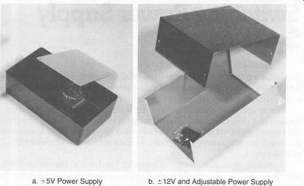
Figure 4-14. Enclosures
a. +5V Power Supply
b. +12V and Adjustable Power Supply
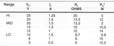
Table 4-4. Resistance Values to Test the Variable Power Supply
* Because of line voltage variations, the P _ values may be different. If P, becomes too high, the thermal protection circuit may shut down the regulator.
SUMMARY
This SECTION has given the design and construction details of three different power supplies that are adequate for a variety of uses. The circuits may be changed or modified as needed by the person building them.
The discussion so far has focused on linear power supplies. In the next two SECTIONs, the basic principles of switching power supplies will be investigated.
Prev: SECTION 3 Basic REGULATED POWER SUPPLY SYSTEMS
Next: SECTION 5 SWITCHING POWER SUPPLY SYSTEMS
Building Power Supplies (Article Index)
Also see:
Link |