This SECTION describes the operation of a switching power supply system which uses switching regulators. A switching regulator has much higher efficiency than the linear systems described in the first four SECTIONs.
Linear series-pass regulators convert an input voltage that is higher than needed to a desired lower voltage. The extra energy (the voltage drop across the control element times the current flowing through it) is dissipated as heat.
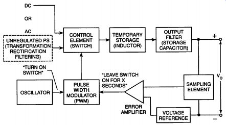
Figure 5-1. Switching Power Supply Block Diagram
As a result, typical series-pass regulators have a conversion efficiency (Poyr/ Pix) of 50% or less.
Switching regulators, on the other hand, can have a conversion efficiency of 85% or more. Such efficiency results in lower power dissipation and much smaller size components for a given power output. Other advantages are:
1. operation over a wide range of current and voltage, 2. switching-mode operation for the control element, 3. input voltage can be lower than the output voltage, and 4. the output voltage can be of opposite polarity than the input voltage.
SWITCHING POWER SUPPLY OPERATING PRINCIPLES
Figure 5-1 is a block diagram of a switching regulator power supply. As one can see, there are many similarities between switching systems and the linear systems discussed in SECTION 3. The differences lie in the action of an inductor used for temporary energy storage, and how the control element is controlled to provide regulation.
Control Element
Action In linear systems, regulation is accomplished by varying the resistance of the control element. In switching systems, it is done by rapidly turning the control element on and off, and by varying the ratio of ON time to OFF time. Unlike the series-pass control element, there is no linear operating state; the control element is either completely on or completely off.
The ON switching action "pumps" energy in sudden bursts into the inductor temporary storage element. During the time that the switch is OFF, the stored energy is directed by a diode into the filter capacitor to supply the load as needed. The sampling element, reference-voltage source, and error amplifier work in an identical manner to those in a linear supply. However, the output of the error amplifier is used differently.
Error Amplifier, Oscillator and PWM
The new circuits for the switching regulator are the oscillator, the pulse-width modulator (PWM), and the temporary storage element inductor. The control element is still a transistor or power field-effect transistor, but it is operated as a switch. It is turned on and off by the PWM as shown in Figure 5-2.
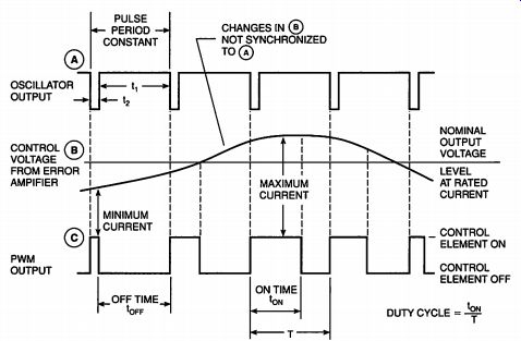
Figure 5-2. Switching and Control Waveforms
The oscillator provides output pulses at a constant frequency, and the PWM output pulses have varying ON times compared to the total period, T, of the oscillator pulses. The oscillator pulse to the PWM input tells the PWM output pulse to turn the control element ON. The error amplifier voltage level tells the PWM how long the output pulse should keep the control element ON.
Thus, the error amplifier output controls the width of the PWM pulse, which controls the ON time of the control element. The duty cycle of the control element is t,y/T.
Inductor Action - Storing Energy
The switching regulator cannot be understood unless the action of the temporary storage inductor is understood. Figure 5-3a shows an inductor in series with resistor, R, which represents the load, and switch, S1, across a battery with voltage Vy. The initial conditions are: S1 is open, current is zero (I=0), and voltage across the load is zero ( V_s=0). The inductor, L, is assumed to have no resistance. The curve shown alongside the circuit plots the value of V_s against time.
Since Vg=IR and R is a constant, the curve also represents the value of I in the circuit at any instant in time. After S1 is closed a relatively long time, notice that Vi = Vin and I = Vin/R.
At the instant that S1 is closed, the current in the circuit tries to increase to the V,y/R value, but the inductor action resists current change. It does this by developing a counter voltage, V _ across itself that is in a direction to resist the current change. The counter voltage is expressed by engineers as the counter electromotive force (CEMF). (This is the same "voltage by induction" that was discussed in SECTION 1 for generators and transformers.) As the current changes, the magnetic flux extending out from the inductor as a result of the current change, cuts the turns of the inductor coil and induces the counter voltage, V _ in the inductor. The V, (or CEMF) developed across the inductor can be expressed by the equation:
v = LAL At where: L = the inductance in henries Al = change in current in amperes At = time period in seconds of current change
At the instant that S1 is closed, the current is trying to change from zero to maximum, therefore, V, is maximum. Since all the input voltage appears across the inductor, V_s=0. As time passes, the current increases in a logarithmic curve as shown for V_s, and finally reaches its maximum value, V,y/R. When the current reaches maximum, it no longer changes, and the magnetic flux stops changing; therefore, V,=0. Since all of the input voltage, V,y, appears across R, Vy is maximum. Thus, the action of the inductor is to resist a current change and store energy in the magnetic flux field built up around it by the current through it. A similar opposition to current change that occurs when S1 is opened is described in the following paragraphs.
Inductor Action - Releasing Energy
Figure 5-3b is the same circuit as Figure 5-3aexcept diode, D1, has been added.
The diode's purpose will be explained shortly. The current in the circuit is maximum, V,y/R, and Vy=V,y. Energy has been stored in the magnetic flux surrounding the inductor. Now, S1 is opened.
The curve alongside the circuit plots V against time. At the instant S1 opens, the current, I, wants to change to zero because S1 is open. Since I wants to change to zero, the magnetic flux field built up in L collapses. As the magnetic flux cuts the turns of wire in the inductor, the counter voltage, Vi, is again induced, but this time the polarity of V, is opposite to what it was in Figure 5-3a.
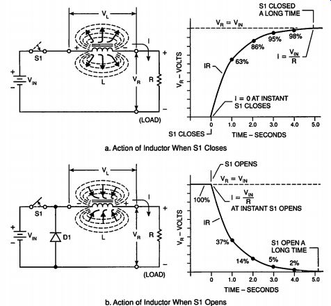
Figure 5-3. Switched Inductor Action. a. Action of Inductor When S1 Closes
; b. Action of Inductor When S1 Opens
The polarity is such that it wants to keep the current in the same direction as it was before S1 opened. D1 provides a complete path for I through Rand Las the magnetic field collapses. (If D1 were not present, a very high voltage would be developed across the opened S1 contacts, causing the contacts to arc over to release the stored energy in L.) Thus, the energy stored in the magnetic field of L is returned to the circuit by inducing a voltage in L to resist the change in I, and to keep I through R in the same direction it was before the current change occurred. Vi, and thus I, reduces along a logarithmic curve as the field collapses until I and V_s are zero.
V is calculated from the same equation as for Figure 5-3a. The inductor action described in Figures 5-3a and 5-3b is used in several different types of switching regulators.
STEP-DOWN REGULATOR
Figure 5-4a shows a control element, inductor and output filter for a step-down switching regulator. It is used when the required regulated voltage is lower than the input voltage. When the control element is switched on, the inductor stores energy, helps supply load current, and supplies current to the capacitor.
When the control element is switched off, the energy stored in L helps supply the load current, but also again restores the charge on C; that is supplied to the load during the time that the control element is off and L has discharged its energy. In this circuit V, =V,y-V, when the control element turns on, and V,=V, when the control element turns off.
Alongside the circuits in Figure 5-4, waveforms of inductor and/or capacitor currents in the circuits are plotted against the time that the control element is on and off. Figures 5-4a and 5-4b show curves of the current, I, into the output filter capacitor. There are times when L is supplying current to charge the capacitor (+1) and supplying the load current as well; and there are times when the load current is supplied only by the capacitor (-I¢). The switching regulator, when working properly, is just at balance in a switching cycle-it is supplying the capacitor as much charge, +Q, as the load discharges, -Q, from the capacitor.
STEP-UP REGULATOR
Figure 5-4b shows the same circuit parts for a step-up switching regulator. It is used when the required regulated voltage is higher than the input voltage. It operates slightly differently than Figure 5-4a. Energy is stored in L when the control element is on. The energy is supplied by Vjy and V, =V,y during this time.
The load, isolated by D1, is supplied by the charge stored in C;. When the control element turns off, the stored energy in L is added to the input voltage, and I, helps supply the load current and restores the energy discharged from Ce. Cr supplies current to the load after L discharges. When the contrpl element turns off, V.=V,-V _.
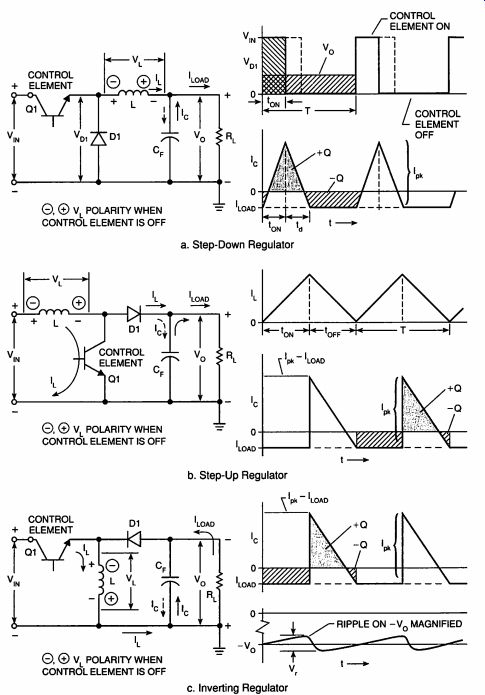
Figure 5-4. Types of Switching Regulators
a. Step-down Regulator
b. Step-Up Regulator
c. Inverting Regulator
INVERTER REGULATOR
Figure 5-4c shows the same circuits parts for an inverter regulator, sometimes called a flyback regulator. The inverter regulator is used when a regulated output voltage of the opposite polarity of V,y is required. Its operation is similar to the step-up regulator. When the control element is on, energy is stored in L, and D1 isolates L from the load. The load current is supplied by the charge on Cr. When the control element turns off, the stored energy in L charges Cto a polarity such that V, is negative. I, supplies load current and restores the charge on C; during the time it is discharging its energy. As with the step-up regulator, Ce supplies the load current after L discharges. When the control element is on, V_.=V}y; when the control turns off, V, =V _. Depending on how the inverter is designed, it can be used for voltages higher or lower than the input.
COMPLETE SWITCHING REGULATOR
Figure 5-5 shows a functional block diagram of a complete step-down switching power supply. Each of the individual functions will be discussed in more detail.
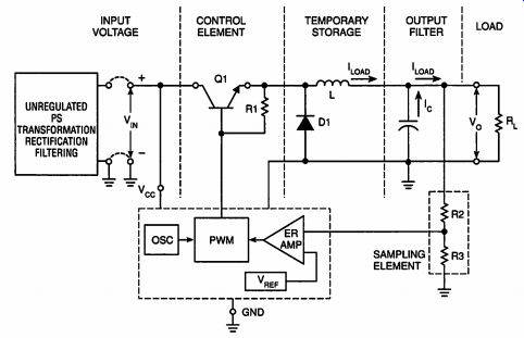
Figure 5-5. Complete Switching Regulator (Step-Down)
Input Voltage
The input voltage for a switching power supply can vary over a surprisingly wide range while still maintaining good conversion efficiency. An ac source is indicated for Vy. All the same design considerations apply for the transformation, rectification and filtering as for the unregulated supply of SECTION 2. The ripple voltage filtering, which takes care of any 60Hz or 120Hz noise, can be somewhat less because of the output filtering of the switching regulator.
Control Element Switch
The control element switch is a switching power semiconductor. It must have low Vy, across it, and must have fast switching times. It may be a single NPN transistor or power FET, or it may be a combination NPN and PNP for higher gain operation. Regardless of what type of transistor is used, it is turned completely on (lowest resistance) during the ON time, then abruptly turned completely off (highest resistance) during the OFF time. It is used as if it were a relay, but operates at a very fast rate-from 20kHz to 100kHz. A 100 kHz wave has a period of 10 microseconds (0.00001 second).
The Catch Diode - Directing the Energy
When the magnetic field of the inductor begins to collapse and release its stored energy, the energy must be contained and channeled in a useful direction. A diode, called the catch diode, does this in each of the circuits of Figure 5-4. It directs the stored energy into the output filter capacitor. The one-way conduction of the diode is used to provide the proper circuit connection when the induced voltage across the inductor is the proper polarity. Due to the high switching frequencies in these supplies, the diode must have a very low for ward voltage and a very fast switching time and recovery time. A Schottky diode is an ideal diode for the application.
The Inductor
The action of the inductor has been discussed thoroughly. The main concern is that the chosen inductor has the proper inductance, that it not saturate during its operation, and that the core has the volume to handle the power required. If it saturates, it loses its inductance and its ability to efficiently transfer energy to the output.
The inductance is determined by the core material and the number of turns of wire on the core. Ferrite and powdered iron cores are usually used for switching power supply inductors. When iron laminated cores are used, they have core loss at higher frequencies which causes the supply efficiency to be low.
The inductance of a coil can be determined from the following equation:
1 = N°Auu, 1 where: L = inductance in henries N = number of turns A = cross sectional area of coil (m?) u = permeability of core material u, = absolute permeability of air (1.26 X10? H/m) 1 = length (m) Inductance increases with more turns, larger area, higher permeability, and shorter length.
Filters
The output filter capacitor serves essentially the same function in the switching regulator as it does in the series-pass regulator; that is, it stores energy to be used by the load. Because the output ripple frequency is much higher, the output filter capacitor usually is a much smaller value than for the series-pass regulator.
The input filter must reduce the 60Hz or 120Hz ripple to acceptable values and/or it must keep the switching-frequency ripple from the input to keep the system stable and noise free. Switching power supplies can be a significant source of electromagnetic interference (EMI). Shielding and filtering are used to keep any generated EMI from escaping.
Oscillator and PWM Circuit
Refer again to Figure 5-2 where the operation and waveforms of the oscillator and PWM were discussed. A convenient IC for both functions is the 556 dual timer. Figure 5-6 shows the 556 interconnected as an oscillator and a PWM.
The first timer is used as a free-running oscillator, or multivibrator. The oscillation frequency is calculated by the following equation:
_ 1.44 (Ry + 2Rp) Cr
The ON output pulse (C) from the PWM (the second timer) to the control element is triggered on by the constant frequency pulses (A) from the oscillator. When triggered, the PWM output goes high, turning on the control element. The output remains high for a time determined by the control voltage (B) from the error amplifier.
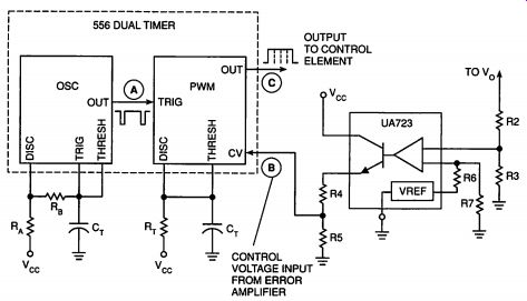
Figure 5-6. Oscillator, PWM and Error Amplifier. OUTPUT TO CONTROL ELEMENT;
CONTROL VOLTAGE INPUT FROM ERROR AMPLIFIER.
When the ON time has expired, the PWM resets the output, forcing it low and turning off the control element. The PWM output remains low until it is triggered again by the oscillator. The time range of the ON pulse is controlled by R; and C, the oscillator frequency by R, and Rs and its C;, and the trigger pulse width by Rs.
Error Amplifier and Voltage Reference
A convenient IC to use for the error amplifier and voltage reference is the 723 regulator described in Figure 3-8, and shown again in Figure 5-6. The sampling element, made up of R2 and R3, delivers a feedback voltage to one input of the error amplifier. The error amplifier compares the feedback voltage to the reference voltage, and produces a corresponding drive current for the 723's output transistor. The output resistors R4 and R5 develop the final control voltage connected to the PWM input. When using the 556 as a PWM, R,=0 because the voltage range of 3.3-10.3V is a convenient range for the 556. If V, of the regulator is greater than the 7.15V reference voltage, the reference voltage can be connected directly to the inverting input of the error amplifier;
however, this restricts the voltage swing of the control voltage. It is best to divide down the reference voltage with R6 and R7 to a lower voltage, and set the voltage on the inverting input from the sampling element to the same value.
DESIGN CHOICES
In any switching regulator design, certain design specifications are set for the design. Using these, the component values and design parameters are calculated and selected for the type of regulator used for the design.
Design Specifications Output Voltage
What nominal output voltage(s) is required by the load? This sets V_o.
Load Current
How much current is required by the load? Sometimes this specification is for small load variations that may occur around a steady-state load current. If the current will not vary from a minimum load to full-load, some of the components may be smaller, or the efficiency higher, etc. The regulator must still be capable of supplying the full-load current.
Regulation
What percent regulation is required by the circuits or equipment to be powered? Some circuits need only 10%, while others need 1%.
Ripple Voltage
How much noise or ripple variation can the circuits or equipment tolerate? This specification determines the quality of filtering required on the regulator output.
Design Parameters
With knowledge of the specifications, the available input source, the available components, and the design flexibility, the regulator type can be selected and the design parameters determined. The following parameters usually are required:
a. Duty cycle and ON time d. Switching frequency
b. Peak current e. Output filter capacitance
c. Coil inductance f. Switching transistor and diode ratings.
Duty Cycle and ON Time
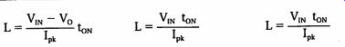
If a step-down regulator is used, in order to support an output of V, from a higher input voltage, V|y, the area under the two voltage-time curves must be equal as shown in Figure 5-4a. Vy X toy must equal Vo XT. Thus, the duty cycle, DC, and ty equations are:
ton _o _ Vo _VoT Vp T TV TT a
The duty cycle and output voltage for three type regulators are as follows.
The equation for V _ of the step-down regulator shows that V, can be controlled by controlling the duty cycle.!
Duty Cycle =
Step-Down Step-Up Inverter V, Vo - V, {Vol Dutv Cvcle LY 0 "IN - vevee Vo Vol +Vx
\Y/ DC Output Vv Vo = VDC Vo = Te {Vol = Vin 1-DC
{Vo} is the value of ~V _ without the sign
Peak Current
The peak current in the switching regulator occurs when the inductor current is just enough to discharge the inductor completely and replace all the charge on the output filter capacitance at maximum load current. It is determined by the maximum load current and the fact that the inductor must be allowed to completely discharge (I, =0). The peak current varies with the different regulators as follows:
Step-Down Step-Up Inverter
V, Ik = 2100p Tox = 2 Iioap ra Ix = 2 Lioap [1 + IN ol
-- Linear Technology Corporation, Application Note 19, C. Nelson, LT1070 Design Manual.
Coil Inductance The voltage across the inductance, L, during the peak current change in time toy determines L. The general equations for the voltage and inductance is:
'Ve L I L= V ton
. ton Lok For the three types of regulators, L is (disregarding transistor and diode drops):2 Step-Down Step-Up Inverter
p=¥n-Vo, L= Un ton L= Vn ton Lox Lox |
Knowing the peak current, toy, and the voltage(s), the inductance can be calculated. The inductance value for continuous current in the inductor is chosen based on the minimum current that the switching regulator must handle-the lower the current, the larger the inductance. Calculate the I, current using the minimum current, and use this value to calculate the inductance.
Switching Frequency
The period, T, must be long enough to allow ty +t,. Using the voltage equation above, the value of t, that allows L to discharge completely must be:
Step-Down Step-Up Inverter
Since T=ty+t, 1/T determines the maximum frequency.
For the project designs of SECTION 6, t _ is between 10 and 20 microseconds, and the duty cycle is set at the midrange of the load current to be regulated, and thus, the frequency is set. t _ will vary as the regulator controls the pulse width, getting narrower as the load decreases. Since the frequency remains constant, t.. increases and exceeds t _ and the inductor, being completely discharged, goes into discontinuous operation. Therefore, if the PWM and error amplifier pulse width versus control voltage curve will allow it, t _ and the frequency are best set when handling the lowest current.
Output Filter Capacitance
Increasing the charge on a capacitor increases the voltage across it; therefore, the I. (and charge) curves of Figures 5-4 would cause a ripple voltage as shown in Figure 5-4c. Since Q=CV, then C=Q/V.
2. Motorola Semiconductor Technical Data MC34163/D "Power Switching Regulators," Motorola Inc., 1990.
As shown in Figure 5-4, the charge added or subtracted from C_ is the area under the I current-time curves. The largest charge deviation is used to calculate the value of C, to limit the voltage change to the specified ripple voltage.
With V, representing the ripple voltage, C. is:
_ AQ Ce= V.
Using geometry to calculate the current-time area (IXt) and considering that the +Q is the same for toy and t, or tog, the equations for C; of the different types of regulators are as follows:? Step-Down Step-Up Inverter
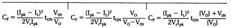
By substituting the voltage specification for V_r the value of C_F can be calculated.
Ratings for D1 and Q1 As stated previously, the diode is usually a Schottky diode because of its excellent switching times and low forward voltage. The diode's PIV need not be greater than the larger of the input or output voltage. It must handle the peak current of the regulator.
The transistor must have low forward voltage and must have a breakdown voltage greater than any output-to-input difference, including polarity. It also must handle the peak current of the regulator, and have switching times much less than any t_on times.
SUMMARY
The ability to build a switching power supply opens the door to a wide range of battery-powered projects that would not be practical with linear regulators.
This SECTION presented the basic operating principles that govern switching power supplies, the basic types-step-down, step-up, and inverter-and their circuits, the calculation of design parameters and the selection of components. SECTION 6 shows how to build some useful switching power supply projects.
--- Texas Instruments Application Report SLVA001, J. Spencer, E.J. Tobaben, "Designing Switching Voltage Regulators with TL497A."
Prev: SECTION 4 LINEAR POWER SUPPLY PROJECTS
Next: SECTION 6 SWITCHING POWER SUPPLY PROJECTS
Building Power Supplies (Article Index)
Also see:
Link |