This SECTION contains two switching power supply projects to demonstrate the basic concepts and fundamentals for designing a switching power supply, not to design the most elaborate and exotic supply. All the parts used are commonly available from Radio Shack.
The integrated circuits used clearly show the selection of major functions, such as oscillator frequency, PWM pulse widths for the trigger and turn-on time pulses, and error-amplifier reference voltage. Major semiconductor manufacturers are now concentrating on integrating all the control functions of the switching power supply for lower-wattage power supplies into one IC.
DESIGN PARTS, LIMITATIONS AND CAUTIONS
Table 6-1 lists specifications for the ICs, semiconductors and inductors used for the projects. These specifications place boundary conditions on the project designs.
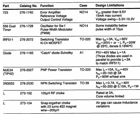
Table 6-1. Project Parts and Their Design Limitations
ICs For the projects, Vjy =+12V to meet the V requirement of the 723. Feedback resistors are used to limit the gain of the 723, even so, some manufacturer's parts seem to cause the closed loop operating point to be right at the edge of the range of the voltage swing. Some 556 dual timers multiple trigger and cause misoperation. A calibration procedure has been setup in SECTION 7 to assure proper closed-loop operation. This procedure should be followed before applying power to the switching power supplies.
Transistor and Diode
Note that the power FET, IRF511, used for switching has a maximum I,s=3A, while the maximum collector current of the MJE34 is I.=10A. However, the design limitation is the peak inductor current that can be switched through the Schottky diodes. Even though it is not the best design technique, three Schottky diodes are operated in parallel to provide the same 3A maximum switching current as the IRF511. This is not normal design practice because, at the maximum peak current of 3 amps, the diode with the lowest V_s tends to "hog" more current than the other two, which exceeds its individual current rating, If a diode fails, it usually shorts because of excess current, which protects the other diodes in parallel. A 1N5822 Schottky diode is an alternate choice if the Radio Shack part is not available.
Inductor
Readily available inductors from Radio Shack, though not the most efficient inductors, provide practical design examples. The 100uH RF choke has a continuous current rating of 2A; however, switching 3A at the step-down duty cycle provides satisfactory operation. The snap-together choke core was glued together with steel-filled, conductive epoxy cement before the coil was wound on it. Nova Magnetics wound a special 170pH inductor for a step-down design.
Its core and coil specifications are given in the Appendix, as well as a list of other magnetic materials manufacturers and distributors.
Maximum Load Current
The maximum load current that can be drawn from the project designed power supplies can be limited by:
1.The peak current in the inductor, which is limited by the maximum current that can be switched by the transistor and diodes.
2.The maximum current limit of the power supply providing the input voltage (Vin).
Step-up designs demand high currents from the input supply due to the output high-voltage power transfer. The input current to a power supply is calculated using the following power-transfer equation:
_ Vo Xion Vin X Eff IN
Caution---Switching power supplies require a minimum load. If operated with no load, the regulator controller will decrease the PWM turn-on time to very narrow pulses, causing very high voltages from the inductor which will destroy the switching transistor, diodes, and possibly the other ICs. In addition, the discontinuous inductor operation on turnoff causes unstable operation and subharmonic frequency generation. A minimum load current limit for the inductance used is specified for each project design. A commercially available switching power supply may have an internal active load that draws the minimum current from the supply if there is no load on the power supply terminals. When an external load is placed on the supply that exceeds the minimum current, the active load cuts out, and is effectively removed from the circuit.
PROJECT #1 - STEP-DOWN CONVERTER +12V TO +5V
Project #1 is a regulated +5V supply to power digital logic circuits in an environment, such as an automobile, where the only available power source is approximately 12V dc. The circuit schematic is shown in Figure 6-1.
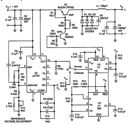
Figure 6-1. Step-Down Converter Circuit +12V to +5V
Design Specifications Vin = +12V Input Regulation = 2% for a =5% Vo = +5V input variation (Loaomax) = 1.5A Switching Frequency = approx. 50kHz l.oappiny = 300mMA
Ripple = 50mV at I _ = 1A Load Regulation = 2% for |, Current Efficiency = 65% @ lop = 1A range Operating Ambient Temperature = 25°C
Input Voltage and Its Supply
The adjustable linear supply designed in SECTION 4, with a maximum load current limit of 1.54, is used to supply Vy. A regulated input supply simulates a +12V battery, eliminates V,y variations, and makes it easier to build a successful, stable switching power supply. For an application other than + 12V, the reader need only design an unregulated input supply to handle the load current variations expected.
Output Voltage
The +5V output is regulated to 2% over the load current range. The 2% regulation is maintained for an input voltage variation of +5%.
Load Current
Using the input current equation and the equation for step-down peak current from SECTION 5 (calculations are shown in Table 6-2), the load current limit for the step-down design is 1.5A because the inductor peak current of 3A cannot be exceeded due to the Schottky diodes. The power supply efficiency was assumed to be 65%.
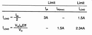
Table 6-2. Load Current Limits
With transistors and diodes that have higher current ratings, the load current could increase to 2.34A before the I _=1.5A limit is reached.
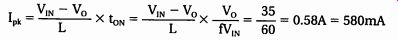
Minimum load current is determined by the inductance used in the circuit. Since the design uses a 100pH choke and f =50kHz, the peak current at the minimum output load current can be determined from the equations in SECTION 5 as follows:
-----------
Since I, = 21, psp, minimum I, _;, = 290mA.
The switching power supply regulates below the minimum current, but the inductor begins to operate in discontinuous mode, which generates more noise and is more difficult to stabilize.
Oscillator
The oscillator is one section of the 556 dual timer IC operating in an astable mode. C12 is the timing capacitor. The total series resistance of R14+R15 and R16 charge the capacitor during the time, t, shown in Figure 5-2, when the output is high, and R16 discharges the capacitor during the time, t _ when the output is low.
The basic operating frequency of this supply is 50kHz, with a period, T, of approximately 20us. The trigger pulse width, t _ is slightly larger than 1ps. The trigger pulse width is initially calculated using the equation t,=0.693 (R16)(C12), and the frequency using the equation f=1.44/[R14+R15+2(R16)](C12), as given in SECTION 5.
According to the equations, f=94kHz using the final component values, and t,=0.693us. Internal delays of the 556 IC itself cause the equation to yield only approximate values. The final circuit values shown in Figure 6-1 were determined experimentally using an oscilloscope to monitor the waveform.
Pulse-Width Modulator
The PWM half of the 556 is used in a "one-shot" configuration, where it produces a single positive pulse for every negative-going trigger pulse it receives from the oscillator. The width of the PWM output pulse depends on the values of C11 and R13, and on the control voltage. Without a control voltage on that input, toy=1.1(R13)(C11), or 11ps. The resistor and capacitor establish the range, and V _ from pin 10 of the 723 to the control voltage input to the 556 (pin 11) determines the exact pulse width. The output from the PWM section of the 556 (pin 9) drives the base of an NPN transistor in the switch circuit. Again, the equations predict approximate values; the values shown are determined experimentally.
Error Amplifier and Voltage-Reference
The switching power supply projects use the 723 regulator IC as the error amplifier and voltage reference. The 723's built-in current-limit circuit is not used. Pins 2 and 3 are left unconnected.
In this project, the output voltage is fed back directly to the inverting input of the error amplifier, pin 4, as illustrated in Figure 6-1. The reference voltage output is connected through a voltage divider (R7 || R8) and (R9+R10+R11) to the non-inverting input of the error amplifier. R10 and R11 form a reference voltage adjustment used in the closed loop calibration procedure to adjust the output voltage of the regulator to +5V. The voltage of the non-inverting input to the 723 should be within 0.01V to 0.03V of +5V. A 0.05uF capacitor is connected between V _ and the non-inverting input of the error amplifier to stabilize the error amplifier against noise feedback from Vy.
To improve the regulation stability, a network consisting of a total of 630 PF (a 220pF and a 470pF) in parallel with a 1-M-ohm resistor is connected between the inverting error-amplifier input, pin 4, and the frequency-compensation input, pin 13. Both resistor and capacitor values were determined experimentally. Circuit layout can affect stability. False triggering and erratic output voltage under load are signs of unstable circuits. Keep all connecting leads as short as possible.
The error amplifier output from the 723 is an emitter follower. The emitter, pin 10, drives a 470 ohm resistor connected to ground to supply the control voltage to pin 11 of the 556 PWM. This voltage ranges from 3.3V to 10.3V depending on the setting at the non-inverting reference input, the sample-voltage input, and the reference voltage. The midpoint output current condition of the design should set this voltage at about 7V. The collector of the internal output transistor, Vy, is tied to Vc and the input voltage V_sy. A 0.1uF ceramic capacitor across Vcc reduces the effects of power-supply noise.
Inductor Choice
Using, f=50kHz, toy is determined from the duty-cycle equation in SECTION 5 as:
fo = Vo _ 5 NTUOfV, 50 X 10° X 12
The inductance required for a peak current of 3A is calculated from the step-down equation in SECTION 5, as follows (f=50kHz):
12-5 5 3 50 X 10% X 12
An inductance of 19.4pH is the minimum inductance that can be used at a peak current of 3A at 50kHz. The minimum current of 290mA for continuous mode operation using the 100pH choke was calculated using the same equation. 100puH is used so the minimum current can be at least 300mA. If a lower minimum current is required, a larger inductance must be used. The size of the inductor may affect the overall size of the power supply in many designs.
= 8.33us L= = 19.4uH
Switching Transistor Choice
An MJE34 PNP power transistor is chosen as the switch because of its low Versar- The PNP transistor has its emitter tied to Vyy=12V. It is turned on by pulling 150mA of base current through a 50-ohm resistor to ground. To ensure a rapid turn-off time, a 10 ohm resistor is connected between the base and emitter, providing approximately 70mA of turn-off current. The total base plus turn-off current is limited to approximately 220mA by the series 50-ohm resistor, composed of two 16 ohm, 1W resistors in parallel for extra power handling capability.
Since the output waveform of the PWM is high during the on time of the switch, the signal needs to be inverted from the PWM before driving the base of the MJE34. A small-signal NPN transistor, the 2N3053, inverts the PWM output and drives the base of the MJE34. The PWM output drives approximately 30 mA into the 2N3053 base through a series 220 ohm current-limiting resistor. A 33 ohm resistor from the base to ground provides 21maA of turn-off current to ensure rapid turn-off time.
"Catch" Diode Choice .
The Schottky-barrier diode is rated at 40 volts peak repetitive reverse voltage, and will handle an average forward current of 1A. Three diodes are used in parallel to provide 3A. This is a weak link in the design, but was done to demonstrate that the rest of the circuitry could handle 1.5A.
Output and Input Filters---To keep the output ripple voltage (V,) below 50mV, the minimum output- capacitor value is calculated using the step-down equation for C; from SECTION 5.
With I,=3A, I, =1.5A and t;y=8.33us, the minimum C; for this supply is:
(3 - 1.5)? 12 2X0.05X3
A small size, 1000uF, 16V electrolytic capacitor with radial leads, almost 10 times the size needed, is selected for C.. A 0.1uF, 50V ceramic capacitor is placed in parallel to bypass high-frequency noise.
A 220pF, 35V input capacitor acts as an input filter. It is necessary in a switching power supply because the switching action of the transistor can induce a hefty ripple voltage on the input supply voltage.
Construction Details---The project is built on a 1%" X 6" strip of perfboard (RS# 276-1396). This allows the same circuit layout of Figure 6-3 to be included on one end of a circuit board for an application that is to be powered by the supply.
Component Layout
The component layout, while originally hand wired on perfboard, can be used as a guide for making a printed circuit board using a PC-board kit (RS# 276 1530). As shown in the photographs in Figure 6-2, power and ground conductors were made from 20-gauge hookup wire, with wire-wrap posts used to connect between the circuit side and component side of the board. Smaller wired connections were made either with wire-wrap wire or by bending the component leads into the desired shape after insertion into the board.
Figure 6-3 shows a parts-placement and wiring diagram from the component side and the circuit side. The component leads and wiring on each side of the board are shown as solid lines. The parts used are listed in Table 6-3.
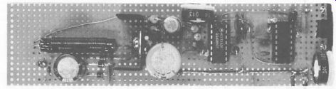
Fig. 6.2
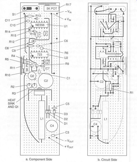
Figure 6-3. Parts-Placement and Wiring Diagram. a. Component Side b. Circuit
Side
Operation and Testing
A calibration procedure is included in SECTION 7. Check out your total circuit carefully and assure that all connections are correct. Make sure that you apply no power to your circuit until you perform the calibration procedure. Because of component tolerances, values stated in a design may vary due to the combination of tolerances present in the circuit.
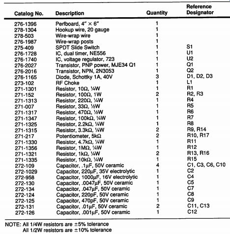
Table 6-3. Parts List for Step-Down Converter
NOTE: All 1/4W resistors are +5% tolerance
All 1/2W resistors are *10% tolerance PROJECT #2 - STEP-UP CONVERTER +12V to +24V
An application that is well served by a switching regulator is when a dc output voltage is required that is higher than an input dc voltage. Project #2 is a regulated +24V supply that has an input voltage of +12V. It is a design that demonstrates a basic step-up converter circuit, and shows some of its advantages and limitations. The schematic is shown in Figure 6-4.
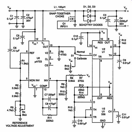
Figure 6-4. Step-Up Converter Circuit +12V to +24V Design Specifications
Vy = +12V Input Regulation = 2% for a =5% input Vo = +24V variation loacimaxy
= 750mA t Switching Frequency = 41kHz LOAD(MIN) = 200mA Ripple = 100mV at
- = 0.6A Load Regulation = 2% for | op current Efficiency = 30% range Operating
Ambient Temperature = 25°C
* limited to 675 mA by input supply (90% eff.)
Tlimited by 3A maximum switching current (100% eff.) Input Voltage and Its Supply The input power supply is again the linear adjustable supply of SECTION 4 with its 1.5A maximum load current limit.
Output Voltage
The +24V output voltage is regulated to within 2% over the output current range, and over a +5% variation in input voltage.
Load Current
Since the input supply can provide no more than 1.54, it limits the load current that can be drawn from the step-up converter. As a result, the maximum load current is limited to 0.675A, assuming 90% efficiency for the power supply. The calculations are shown in Table 6-4. If an input power supply is used that can supply more than 1.5A, then the load current could increase to 0.75A before the peak inductor current limit of 3A is reached.
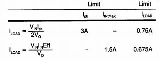
Table 6-4. Load Current Limit
The inductance used for project #2 is a 200uH coil wound with 18 turns of #22 magnet wire on the snap-together toroidal core. The minimum load current for this inductance, based on a frequency of approximately 41kHz, and a duty cycle of 0.5, is 180mA based on the following calculations:
12 Vin =N wp =e Cx 12 X 10° = 0.72A Pk, tox = 300 x 10°
Substituting 0.72A in the Io, equation in Table 6-4, I oxp (nay = 180mA.
Oscillator
The 556-based oscillator/PWM circuit is identical to that of the step-down converter with some of the values changed. The values for the step-up converter are as follows:
R14 in parallel with R13 = 20 k-O
R15 = 1.0 k-O
C10 = 0.001pF
The resultant frequency is approximately 41kHz.
The trigger pulse width is slightly larger than 1us.
Pulse-Width Modulator The output from the PWM section of the 556 (pin 9) drives the gate of the IRF511 power FET. The values for the resistor and capacitor are as follows:
C9 = 0.01uF R12 = 1.0 k-O
The ty, time for median pulse width is 12us.
Error Amplifier and Voltage-Reference Choice
The error amplifier and voltage reference is provided by the 723 regulator as in the step-down converter. Since the output voltage that must be sampled is greater than 7 volts, the error amplifier circuit shown in Figure 6-4 differs slightly from that of the step-down converter. The sampling element is an additional voltage divider from V, with the junction of R8 and R9 providing the sampled voltage to the inverting input of the 723. When the output is at 24 volts, the voltage at the inverting input is from 5.85 to 5.95 volts. The reference voltage is divided down to approximately 5.90 volts at the non-inverting input by the voltage divider formed by resistors R1 through R5. Three circuit design techniques assure regulator stability. First, a 0.1uF capacitor is connected from Vy to the non-inverting input, pin 5. Second, a 690pF capacitor in parallel with a 220 k-O resistor are connected between the error-amp input, pin 4, and the frequency-compensation input, pin 13. Third, a 0.1uF ceramic capacitor is placed from V_ to ground to reduce the effects of power-supply noise.
Pin 11, the collector of the internal output transistor is tied to Vy, and the emitter drives a 470 ohm resistor connected to ground. This is the control voltage that varies the PWM output.
Inductor Choice
I, is again limited by the Schottky diodes to 3A, and is used to determine the minimum inductance as follows:
\'/ 12 L=--X ty =- X12 X 10° = 48uH Lox 3
Only 48uH are required when the power supply operates at maximum inductor current, but the 200pH value is chosen to allow the regulator to operate at a minimum current of 180mA. If a lower minimum current is required, the inductor would have to be larger.
Coil Fabrication
The two ferrite halves of the snap-together core are glued together using a steel-filled, conductive epoxy cement. Electrical tape is wrapped around the core before the #22magnet wire is wound evenly on it. The completed inductor is shown in Figure 6-6c.
Switching Transistor Choice
An IRF511 power field-effect transistor (FET), rated at Ig ,. _=3A continuous, is used as the switching transistor in the step-up design. The breakdown voltage is 60V, well above the levels encountered in this supply. The power FET has a maximum forward voltage drop of 1.8V at the peak current of 3A. The input capacitance of a power FET is relatively large. The 556 has a totem-pole output stage that rapidly charges and discharges the IRF511 input capacitance, ensuring fast turn-on and turn-off times.
"Catch" Diode Choice
Three Schottky barrier diodes are used in parallel to handle a peak inductor current of 3A, even though the maximum load current of 1.5A from V, limits the maximum inductor current to 2.7A.
Ge X 12 X 10° X 2 - = 182uF
The actual output capacitor is 10 times this value to minimize output ripple. The 2200uF, 35V, electrolytic capacitor with axial leads has a size, even for such a large capacitance, that fits nicely on the circuit board. Again a 0.1uF, 50V, ceramic capacitor in parallel bypasses high-frequency noise.
Construction Details
This project is again built on 1%%"X 6" strip of perfboard, and is nearly identical in layout and construction to the step-down converter. The same interconnection materials were used.
Component Layout
The component layout is shown in the photographs in Figure 6-5.
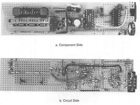
Figure 6-5. Step-Up Switching Power Supply +12V to +24V
a. Component Side
Figure 6-6 shows a parts-placement and wiring diagram from the component and the circuit side. The component leads and wiring on each side of the board are shown as solid lines. The parts used are listed in Table 6-5.
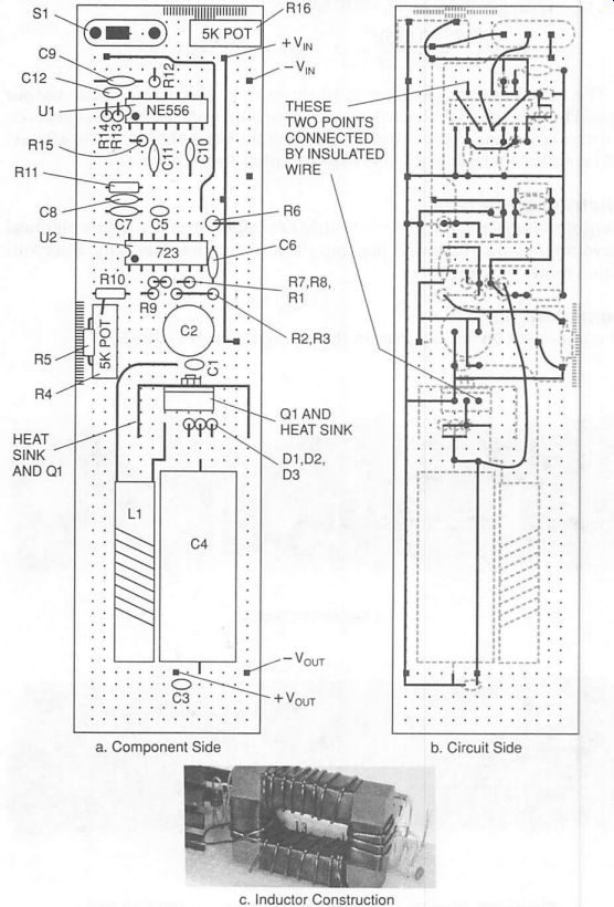
Figure 6-6. Parts-Placement and Wiring Diagram
c. Inductor Construction
Operation and Testing
A calibration procedure is included in SECTION 7. Check out your total circuit carefully and assure that all connections are correct. Make sure that you apply no power to your circuit until you perform the calibration procedure. Because of component tolerances, values stated for a design may vary due to the combi nation of tolerances present in the circuit.
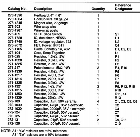
Table 6-5. Parts List for Step-Down Converter
NOTE: All 1/4W resistors are +5% tolerance
All 1/2W resistors are +10% tolerance
Summary
This SECTION concludes the power supply projects. Switching power supply stability can be very sensitive to layout and to the ICs used. Make sure that the calibration procedure in SECTION 7 is followed to assure the regulators will operate properly. In addition, SECTION 7 discusses measurement techniques, presents data on all the project power supplies, and provides troubleshooting tips.
Prev: SECTION 5 SWITCHING POWER SUPPLY SYSTEMS
Next: SECTION 7 MEASUREMENTS, CALIBRATION AND TROUBLESHOOTING
Building Power Supplies (Article Index)
Also see:
Link |