Author: W. Marshall Leach [Assistant Professor of Electrical Engineering, Georgia Institute of Technology Atlanta, Ga. 30332, USA]
THE DESIGN philosophy used in most transistor audio amplifiers today differs substantially from that found in the tube amplifiers of several years past. Aside from the obvious lack of output transformers, the transistor designs differ from the tube ones principally in two ways.
First, most transistor amplifiers are d.c. coupled, at least in all internal stages. This has been made possible mainly by the availability of complementary transistors (i.e. NPN and PNP). There are no such equivalents in vacuum tube circuits. Second, in transistor amplifiers, a much larger amount of negative feedback usually is applied around the amplifier (i.e. from the output to the inverting input) in order to reduce distortion produced by nonlinearities to virtually un measurable levels. The negative feedback typically used may be as high as 40 to 60 dB. Such high levels are so effective in reducing nonlinear distortion that many designers have intentionally designed certain distortions into the "open-loop amplifier." For example, the final output stages of many amplifiers are operated class C (i.e. with no bias current) in order to obtain almost absolute thermal stability without the need for complicated thermal compensation. In such designs, the driver transistors drive the speakers for the first 0.1 to 0.4 volts, and the output transistors switch in above that level. The crossover distortion created by the switching of the output transistors can be neatly "covered up" with the application of sufficient amounts of negative feedback.
For the typical closed-loop gain of 26 dB, 40 to 60 dB of negative feedback requires an open-loop gain of 66 to 86 dB. Such high open-loop gains are easily obtained with relatively few transistor stages (normally two to three stages of voltage gain plus the current gain in the driver and output stages). Some of the latest amplifier designs have made use of high-gain, integrated-circuit (IC), operational-amplifier input stages. A single IC can replace the input stages of both channels is a stereo amplifier and provide the necessary open-loop gain for ultra-low distortion by conventional measurement techniques.
In order that an amplifier not oscillate when the negative feedback loop is connected, designs with a high open-loop gain require careful frequency compensation. The technique that is most often used is called lag compensation. It is given this name because it is accomplished by the addition of capacitors in the circuit which increase the phase lag in the amplifier at the higher frequencies. More importantly, lag compensation also reduces the open-loop gain of the amplifier at the critical high frequencies at which it would tend to oscillate. This tendency toward higher open-loop gains with attendant heavy feedback and lag compensation has led to the identification of a new distortion mechanism called transient intermodulation (TIM) distortion [1, 2]. TIM distortion sounds like crossover distortion, however, it cannot be detected with conventional sine-wave measurements. Indeed, there are presently no standards covering its measurement! TIM distortion occurs principally during loud, high-frequency passages in the reproduced signal, and recent investigations have shown that the ear is very sensitive to it [3]. Basically, it is an overload phenomenon that is caused by heavy feedback in the amplifier.
Tube amplifiers have been traditionally designed with much lower open-loop gains than their transistor counterparts of today. Indeed it was unusual to find open-loop gains higher than 46 to 51 dB in even the best tube amplifiers. For a closed-loop gain of 26 dB, this range of open loop gain requires only 20 to 25 dB of negative feedback.
With such relatively low levels of feedback (by the standards of today), quality tube amplifiers were necessarily designed for minimum distortion and maximum bandwidth before the addition of feedback. Consequently, TIM distortion was never identified as a distortion mechanism in tube amplifiers. (The author has measured a negative feedback of only 5 dB in a popular 10-watt monophonic tube amplifier from the late 1950s. A high-quality, 80-watt stereophonic tube amplifier of the early 1960s was advertised to have a negative feedback of only 22 dB.)
There has been much controversy over what has been called "tube versus transistor sound." It has been suggested by many who can detect the difference that the reason some transistor designs sound "harsh" compared to tube designs is because tubes overload more "gracefully" than transistors do. Whether this explanation is valid or not, TIM distortion must be considered a major reason for the difference in sound. This is particularly true for the cases in which continuous sine-wave tests indicate that a transistor amplifier has less distortion than a tube amplifier, however, the tube amplifier sounds "cleaner" than the transistor one does. Invariably, the transistor design can be shown to have a very high open-loop gain with attendant heavy feedback and lag compensation. Transistor designs with integrated circuit input stages can be particularly susceptible to TIM distortion since so many integrated-circuit operational amplifiers have such a poor open-loop bandwidth after they are frequency compensated for stability. (The very popular 741 IC operational amplifier with internal frequency compensation has only a 2-5 Hz open-loop bandwidth and an open loop gain of 100-105 dB.) The purpose of this paper is to discuss the causes and cures of TIM distortion in transistor amplifiers. Preferred circuit design techniques which minimize TIM distortion will be described. In a later paper, an amplifier which has been designed using these techniques will be described.
TIM Distortion: How Does It Arise?
To understand how TIM distortion is produced, it is first necessary to understand how negative feedback affects the gain of an amplifier. Consider the amplifier modeled in Fig. 1. The model has two input terminals, a non-inverting (+) input and an inverting (-) input, and an output terminal to which the speaker load is connected. The input signal v, is applied to the non-inverting input, and a negative feedback signal v2 is applied to the inverting input. The negative feedback signal is taken from the output of a two resistor voltage divider network connected to the output terminal.
The output signal is given by the product of the open-loop gain of the amplifier times the difference between the signals v, and v2. This is given by the equation
v0 = G(f) [v1 - v2] (1)
where G(f) is the open-loop gain of the amplifier which is a function of the frequency f. In general, G(f) is a complex function of frequency, i.e. it has both an amplitude and a phase. If the feedback signal were zero, the amplifier output signal would equal the product of the open-loop gain times the input signal. However, by "feeding back" part of the output signal to the inverting terminal so that it is subtracted inside the amplifier from the input signal applied to the non-inverting terminal, the gain of the amplifier is effectively decreased. At the same time, the frequency bandwidth of the amplifier is extended, distortion produced by nonlinearities is reduced, and the output impedance of the amplifier is decreased (or alternately its damping factor is increased.)
When the feedback signal v2 is eliminated from Equation (1), it can be shown that the output signal is related to the input signal by the equation
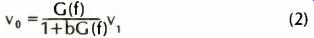
In this equation, b is the feedback factor which is given by
b=R1/(R1+R2) (3)
If the magnitude of bG(f) is much greater than 1, Equation (2) can be approximated by the equation
v0 = (1/b) v1 = Gc v1 (4)
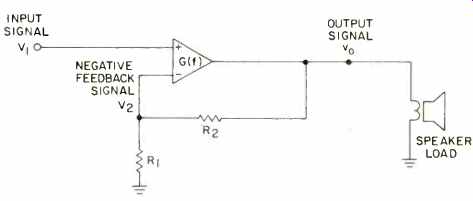
Fig. 1--Model of power amplifier showing non-inverting (+) input, inverting
input (-), and resistive feedback network.
This equation says that if the open-loop gain of the amplifier is sufficiently large, the closed-loop gain is "flat" (i.e. independent of frequency), and it is determined only by the feedback resistors. Most amplifiers are designed with R2 = 19R, which produces a closed-loop gain Gc = 1/b of 26 dB. Equation (4) can be misused if one neglects the fact that it is only an approximation to Equation (2). For any particular amplifier design, there is a frequency above which G(f) decreases toward zero with increasing frequency. This rolloff in the open-loop gain is a natural consequence of the finite bandwidth of the transistors (or tubes) in the amplifier. In the rolloff region, the phase of G(f) can vary rapidly with frequency, leading to serious instabilities in the amplifier when the feedback loop is connected. To insure stability, the circuit designer must verify that in the rolloff region the phase and amplitude of G(f) cannot assume a value such that bG(f) = -1 (i.e. bG(f) has a magnitude of 1 and a phase lag of 180°.) Otherwise, Equation (2) says that the amplifier gain is infinite at the frequency for which this occurs, and this is precisely the condition for an oscillator. In most cases, it can be shown that the amplifier will always oscillate if there is any frequency for which bG(f) has a phase lag of exactly 180° and a magnitude that is equal to or greater than unity. A convenient "rule of thumb" used by many designers says that the phase lag in G(f) should not exceed 135° at the frequency for which the magnitude of bG(f) is unity. Otherwise, the amplifier may oscillate or at best be only marginally stable when the feedback loop is connected.
One convenient way to insure that an amplifier will not oscillate is to design it so that the open-loop gain is decreasing with frequency at a rate of 6 dB per octave at the frequency for which the magnitude of bG(f) is unity. It can be shown that a 6-dB-per-octave gain rolloff can have a maximum phase lag associated with it of only 90°, thus satisfying the above "rule of thumb." This is called lag compensation, and it is accomplished by the addition of capacitors which roll off the high-frequency open-loop gain at the required 6-dB-per-octave rate. This is illustrated in Fig. 2 where the open-loop gain of an amplifier which would oscillate when the feedback loop is connected is sketched versus frequency. Before lag compensation, the open-loop gain is decreasing with a slope of 12 dB per octave or greater at the critical frequency where the magnitude of bG(f) is unity. This critical frequency is that frequency for which the magnitude of the open-loop gain G(f) is equal to Gc, i.e. the closed-loop gain of the amplifier given by Equation (4). After lag compensation, the open-loop gain is decreasing with a slope of 6 dB per octave at the frequency for which the magnitude of G(f) is equal to Cc, thus making the amplifier stable when the feedback loop is connected. The frequency fo defined in the figure is the open-loop bandwidth of the lag-compensated amplifier. This can be considerably smaller than the bandwidth of the uncompensated amplifier. Often fo lies is the range of 1 to 5 kHz for transistor amplifiers. This is considerably less than the bandwidth of audio signals and can lead to the production of strong TIM distortion as will be explained in the following.
In Fig. 2, the closed-loop gain is also sketched to show the effect of negative feedback on the overall frequency response of the amplifier. The negative feedback ratio is defined as the ratio of the open-loop gain Go to the closed loop gain Gc = 1/b, or the difference in these gains when they are expressed in dB. The closed-loop cutoff frequency fc is defined in Fig. 2. In any proper design, fc is larger than the highest frequency signal to be amplified. It can be shown that fc = foGo/Gc for a lag-compensated amplifier.
This equation says, for example, that an amplifier with a 1 kHz open-loop bandwidth will have a 100-kHz bandwidth if 40 dB of negative feedback is used. However, the amplifier would probably be susceptible to very strong TIM distortion.
To illustrate how TIM distortion arises, the amplifier modeled in Fig. 1 is redrawn in Fig. 3 with the diagram broken to show explicitly the transistor stage that is lag compensated. The capacitor that is connected from collector to base of this transistor rolls off the high-frequency, open loop gain of the amplifier at the required 6-dB-per-octave rate to insure that it will not oscillate when the feedback loop is connected. Let us examine the transient response of this transistor stage. Figure 4 shows the signal at point b in Fig. 3 when the signal applied to point a is a voltage step (i.e. an abrupt or instantaneous change in voltage). The voltage waveform at point b is shown for the cases with and without the lag-compensation capacitor. With the lag-compensation capacitor, notice that there is a time delay before the collector voltage can completely attain its final value after the input step occurs. Both this delay and the smoothing of the collector signal shown in Fig. 4 are caused by the lag-compensation capacitor which requires a finite time to charge and discharge after a change occurs in the input signal to the transistor. The same conclusion could be reached by considering the high-frequency gain of the transistor. The lag-compensation capacitor provides a negative feedback path for the high-frequency signal components from collector to base, thus severely attenuating the high-frequency gain. It can be shown that a voltage step contains many high-frequency components. Their attenuation in the lag-compensated transistor causes the time delay and smoothing of the collector output signal.
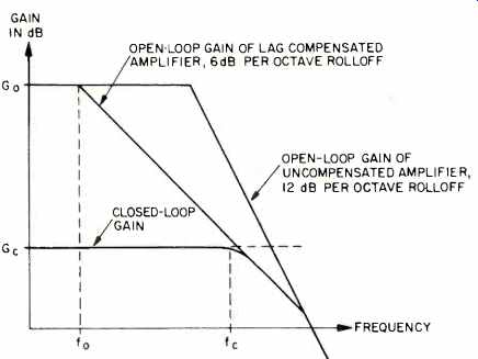
Fig. 2—Open- and closed-loop gains of a lag-compensated amplifier.
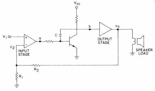
Fig. 3--Amplifier model showing internal transistor stage which is lag-compensated
with the capacitor C.
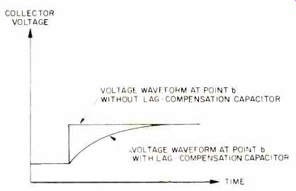
Fig. 4--Response of lag-compensated transistor stage in Fig. 3 to a voltage
step applied to point A.
Now let us consider the response of the amplifier when the voltage step is applied to its non-inverting (+) input. If the open-loop gain of the amplifier were flat and the time delay through it were zero, the voltage step would instantaneously propagate undistorted through the amplifier, back through the feedback loop, and into the inverting (-) input. There it would be subtracted from the input signal, and the difference would be amplified by the input stage to produce the signal at point a in Fig. 3. In this case, the difference signal itself would be a voltage step which occurs at the same time that the input signal does. However, this is not the case when the open-loop gain of the amplifier is not flat and the time delay through it is not zero. When the voltage step occurs, the limited high-frequency response of the lag- […]
[…] mize TIM distortion while providing stability at the same time. Lead compensation is accomplished by connecting a small capacitor in parallel with the emitter feedback resistor of each stage of voltage gain in the amplifier. This is illustrated in Fig. 7 for a typical transistor stage. The value of the lead compensation capacitor is selected to minimize the phase lag in the overall open-loop gain at the critical frequency where the magnitude of bG(f) is unity. Although it is not intuitively obvious how increasing the high-frequency open-loop gain of an amplifier can stabilize it and prevent it from oscillating, lead compensation is a technique commonly applied to stabilize control systems in which an optimum transient response is an important consideration.
In Fig. 8, the open-loop gain as a function of frequency for a lead-compensated amplifier is compared to that for a lag-compensated amplifier which uses a large negative feedback ratio. Notice that the low-frequency, open-loop gain of the lead-compensated amplifier is much less than that of the lag-compensated amplifier. However, as the frequency is increased, the open-loop gain of the lead-compensated amplifier does not begin to roll off until a much higher frequency. Optimally, it should be constant over the entire audio spectrum to minimize TIM distortion. In this particular case, there is a frequency above which the open loop gain of the lead-compensated amplifier is greater than that of the lag-compensated amplifier. For this reason, the resultant closed-loop bandwidth of the lead-compensated amplifier is greater than that of the lag-compensated amplifier. In fact, a lead-compensated amplifier can easily have a closed-loop bandwidth of 1 MHz if it is properly compensated. Although a bandwidth this wide is not necessary for reproduction of audible frequencies, it is usually a natural consequence of lead compensation. Thus, it is desirable to use a passive filter at the amplifier input which has a high frequency cutoff of 20,000 Hz to prevent the application of inaudible high-frequency signals which could overload the amplifier.
An examination of the behavior of the open-loop gains sketched in Fig. 8 in the high-frequency rolloff region will reveal the essential differences between lag and lead compensation. For the lag-compensated case, the open-loop gain is purposely rolled off so that its magnitude is decreasing at 6 dB per octave when it crosses the critical gain level equal to the low-frequency closed-loop gain which is given by Gc = 1/b. In the lead-compensated case, the high-frequency, open-loop gain is allowed to extend to as high a frequency as possible before it begins to roll off on its own.
This rolloff is due to the finite bandwidth of the amplifier, and the roll-off rate is usually 12 dB per octave or in some cases more. In the region where the magnitude of the open loop gain crosses the critical gain level, the lead-compensation capacitors add high-frequency gain so that the magnitude of the open-loop gain is decreasing at a rate of 6 dB per octave at this level. Or equivalently, enough phase lead is added to prevent the phase lag in G(f) from approaching 180° at the frequency where the magnitude of bG(f) is unity.
Thus, in both cases, the magnitude of the open-loop gains crosses the critical gain level with the same slope, and each amplifier will be stable when the feedback loop is connected.
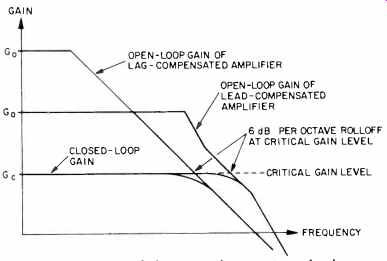
Fig. 8--Comparison of the open-loop gains of a lag-compensated amplifier
and a lead-compensated amplifier.
Since the prevention of TIM distortion requires the use of much less negative feedback than is normally used, it is necessary to avoid certain circuit configurations which have become popular recently. For example, many amplifiers operate with zero quiescent or idle current in the output transistors in order to eliminate thermal drift in the output stage. The driver transistors in these amplifiers drive the speaker through a resistor of 10 to 50 ohms for the first 0.1 to 0.4 volts, and the output transistors switch in above that level. Without the use of a very large negative-feedback ratio, this can produce severe crossover distortion. Thus, the output transistors in amplifiers designed to minimize TIM distortion must be operated class AB, i.e. with a quiescent current usually of 10 mA or more. This requires that the bias current in the output transistors be thermally compensated. Otherwise, they can be destroyed by thermal runaway.
Thermal compensation is usually accomplished with temperature-sensing diodes, which are mounted on the heat sinks with the output transistors and provide thermal feedback to maintain a constant quiescent current in the output transistors.
In summary, the two major design objectives for the prevention of TIM distortion are to design the "open-loop" amplifier for maximum linearity and to design it so that the open-loop bandwidth is at least as wide as the audio frequency spectrum. Both of these require the use of heavy local negative feedback in every stage of voltage gain in the amplifier. This minimizes the need for heavy overall negative feedback from the amplifier output to its inverting input. In addition, local feedback provides the gain reserve in each stage necessary to lead compensate the amplifier for closed-loop stability and maximum open-loop bandwidth.
With an open-loop bandwidth at least as wide as the audio frequency spectrum, the propagation phase delay of high frequency, transient signals through the overall feedback loop around the amplifier is minimized, thus minimizing TIM distortion. We can summarize the most important design considerations to obtain these objectives as follows:
1. All internal stages of the amplifier should operate class A except for the output transistors. These should operate class AB with a sufficient quiescent bias current to completely eliminate crossover distortion in the low-power region. Normally this bias current is 10 mA or more.
2. The input stages should be designed with a sufficiently high bias current in order to minimize their tendency to overload during the high-frequency, transient signals which cause TIM distortion. Since the bias current in the input stages has an important effect on the signal-to-noise ratio of the amplifier, it should not be chosen so high as to degrade the signal-to-noise ratio.
3. All stages in the amplifier should be designed so that each operates "push-pull." For example, this requires a completely complementary design with an NPN transistor for each PNP transistor, and conversely. This significantly improves the linearity of the "open-loop amplifier" and helps to minimize the need for heavy overall feedback to reduce distortion.
4. The driver and power output transistors should be operated in the emitter follower configuration for optimum open-loop bandwidth. In addition, the first driver transistors should be driven from a voltage amplifier stage rather than from a current amplifier stage as is done in most amplifiers which employ a complementary symmetry design.
5. Wide bandwidth transistors should be chosen for each stage in the amplifier, i.e. transistors with a high gain-bandwidth product which is denoted by the symbol fT. Normally, the f is lower for the high-current transistors used in the output stages. Typically, it will be in the range of 2 to 4 MHz.
For transistors used in the lower power stages, available fTs are in the range of 40 to 200 MHz.
6. The overall high-frequency response of the amplifier should be rolled off above the audio spectrum with a passive input filter to prevent overloading by inaudible, high frequency signals. This is best accomplished by connecting a small capacitor or capacitor in series with a resistor between the inverting (-) and non-inverting (+) inputs to the amplifier. In addition, a resistor is placed in series with the input lead to the amplifier. These circuit components roll off the high-frequency, closed-loop gain of the amplifier at a 6 dB-per-octave rate by effectively shorting together the two input terminals at the high frequencies. These components also can improve the amplifier stability in the same way that lag compensation does without producing TIM distortion [1].
Conclusion
TIM distortion is an overload phenomenon which results from the use of a very large negative feedback ratio in audio power amplifiers. It is caused by overloading of the input stages by high-frequency transient signals which experience excessive propagation phase delays in the overall negative-feedback loop around the amplifier. Since it does not occur with steady-stage, sinusoidal signals, it cannot be measured or predicted from standard harmonic or IM distortion tests, for these tests are performed with sinusoidal signals. The prevention of TIM distortion is simple and requires the use of an old design philosophy that proved its validity in the days of the vacuum-tube amplifiers. That is, the amplifier should be designed for low distortion and wide bandwidth without overall negative feedback. Feedback is then added to make a good design better and not to "cover up" problems in the basic amplifier. This design philosophy precludes the use of high-gain, narrow-bandwidth IC operational amplifiers and essentially non-linear circuits, such as class C output stages.
Some of the technical details concerning the causes and prevention of TIM distortion have been presented. It is hoped that the language has not been too technical for the average audiophile nor has it been too over-simplified for the electronics engineer. Those interested in pursuing the technical details further are referred to the excellent work done by M. Otala at the University of Oulu in Finland. Two of his papers are listed in the references.
In an ensuing issue of AUDIO, the complete design of a power amplifier designed to minimize TIM distortion will be presented. The amplifier is a d.c. coupled, completely complementary design which uses 26 dB of negative feedback. A technique for optimally lead compensating the amplifier will be described which makes use of a newly available audio-frequency gain-phase meter manufactured by Hewlett-Packard. At present, this project is behind schedule because of a difficulty in obtaining transistors, some of which have been back ordered for six months.
References
1. M. Otala, "Circuit Design Modifications for Minimizing Transient Intermodulation Distortion in Audio Amplifiers," J. Audio Engr. Soc., vol. 20, no. 5, pp. 396-399, June, 1972.
2. M. Otala, "Transient Intermodulation Distortion in Commercial Audio Amplifiers," J. Audio Engr. Soc., vol. 22, no. 4, pp. 244246, May, 1974.
3. H. Lewitt, et al., "Perception of Slope-Overload Distortion in Delta-Modulated Speech Signals," IEEE Trans Audio Electroacoust., vol. AU-18, pp. 240-247, September, 1970.
( Audio magazine, Feb. 1975; W. Marshall Leach)
Also see:
High-Voltage Amp Design (Feb. 1974)
FTC Power Ratings: An Optimistic View (Feb. 1975)
"I See What You Mean!" How the Westrex 45/45 System Was Adopted by the Record Makers (Mar. 1975)
= = = =