The tunnel diode (TD) is a 2-terminal negative-resistance device that is simpler than the unijunction transistor. It reduces the complexity of some oscillators, amplifiers, flip-flops, and pulse generators. TDs have greatly simplified the design and construction of dip meters. Tunnel diodes are manufactured in a number of types to meet various demands of current, voltage, and power. Operation at frequencies of 2.2 GHz and higher has been attained with TDs.
Tunnel diodes as negative-resistance devices are always operated with forward bias, that is, with anode positive and cathode negative, and must be biased by a low-resistance DC source. Aside from this requirement, their installation and use impose few special demands.
The single prominent short-coming of the TD is its lack of input-output isolation, and this fault probably accounts for its widespread use in many places where it might dramatically simplify circuits.
Before working with TDs, read the hints and precautions in Section 1.
Fig. 6-1. TD basics.
TD THEORY
The tunnel diode consists of a single, specially processed, highly doped PN junction having an extremely thin depletion layer. It takes its name from the fact that current carriers in this device behave as if they tunnel under the barrier, rather than surmounting it electrically, to appear almost instantly on the other side.
This effect is observable at low forward voltage; but at higher voltage, the TD behaves as a conventional forward-biased diode. In the tunneling region, the fast movement of the current carriers enables the TD to be used at very high frequencies and rapid switching speeds. TDs have been made from silicon, germanium, gallium arsenide, and indium antimonide.
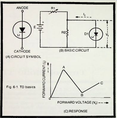
Figure 6-1 (A) shows the
TD circuit symbol.
Advanced mathematics and physics are required for a thorough-going explanation of TD action; however, a simple description of TD behavior can be given with the aid of Fig. 6-1(B) and (C). In Fig. 6-1(B), tunnel diode D1 is forward biased through a voltage divider, R1-R2, operated from the DC supply, E. This is a stiff divider-that is, R2 is very small and f = 1/(6.28VL1 C2) (usually not higher than 10 ohms) and the divider current is high-to prevent R1 from masking the negative resistance of the diode, and to provide good voltage regulation.
As the forward voltage, Vf, is increased by adjustment of R1, the forward current, If, increases from zero, as shown by Fig. 6-1(C), reaching the peak point (A) when Vf is several tens of millivolts. As the forward voltage is increased further, the current decreases from A to the valley point (B). And as the voltage is increased still further, the current again increases, as from B to C.
At the peak point, the current may be a fraction of a milliampere to several tens of mA, depending upon make and model of the diode. The portion of the curve from A to B depicts negative resistance, since here an increasing voltage produces a decreasing current. It is this negative-resistance characteristic that enables the TD to oscillate in a suitable circuit, and also to amplify. The TD is the simplest device that can amplify or oscillate without being DC overloaded.
At very low forward voltage, the diode current results from the tunneling action described above, and increases from zero to A in Fig. 6-(C). After the peak voltage is reached, the current decreases with further increase in voltage, as the tunneling action diminishes (A to B in Fig. 6-1C). And as the voltage is increased still further, normal forward current flows through the diode (B to C and beyond).
GENERAL-PURPOSE AF-RF OSCILLATOR
The tunnel diode permits a very simple oscillator circuit, consisting merely of the biased diode in series with a tuned tank. Figure 6-2 shows such an oscillator, which can operate on either audio or radio frequencies, depending upon the inductance and capacitance of the tuned circuit. The 1N3720 tunnel diode in this circuit is useful to 1.6 GHz.
In this arrangement, the frequency is determined by the values of inductor L1 and capacitor C2. These may be selected with the aid of the following relationships:
L = l/(39.5f2 C2)
C2 = l/(39.5f2 Li)
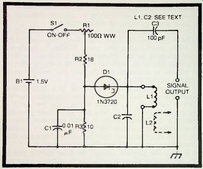
Fig. 6-2. General-purpose AF-RF oscillator.
where in each instance C2 is in farads. L1 in henrys, and f in hertz. In general. L1 will be coreless (or provided with a special HF core of ferrite or other material) for radio frequencies, and will be iron-cored for audio frequencies. Any inductor used in this circuit must have low DC resistance, in order that the negative-resistance characteristic of the tunnel diode will not be affected by this resistance.
The waveform of the output signal is approximately sinusoidal. Simple capacitance coupling is shown in Fig. 6-2.
The 100 pF capacitor (C3) is a good compromise value for AF and RF. But this value may be varied to suit individual requirements. Light loading of the oscillator is imperative for two reasons: to prevent pulling the circuit out of oscillation, and to prevent shifting the frequency.
For these reasons, use the lowest capacitance (C3) that will allow the desired output voltage to be obtained.
The circuit is adjusted by carefully reducing the resistance setting of rheostat R1 to set the TD voltage to a point midway between the peak and valley points on the diode characteristic (see points A and B in Fig. 6-1C). At this point, the circuit will oscillate most vigorously (as shown by an electronic AC voltmeter or similar indicator connected to the signal output terminals) and will also go readily in and out of oscillation as switch S1 is opened and closed.
In this circuit, all fixed resistors are 1/2-watt. Rheostat R1 is wirewound. Capacitors C1 and C3 may be any convenient low-voltage units, but C2 must be of good quality (use silvered mica for radio frequencies) for frequency stability.
If inductive, rather than capacitance, coupling is desired, use a secondary coil, such as L2 shown in dotted lines.
CRYSTAL OSCILLATOR
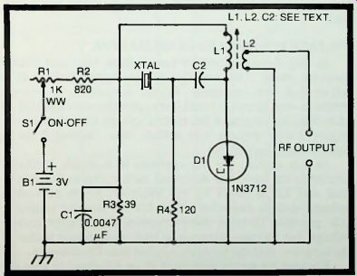
Fig. 6-3. Crystal oscillator.
Figure 6-3 shows the circuit of a TD crystal oscillator employing a 1N3712. This circuit offers good stability and low-impedance output.
In this circuit, the inductance of slug-tuned inductor L1 and the capacitance of capacitor C2 must be chosen for resonance at the crystal frequency:
L1 = 1/(39.5f2 C2)
and
C2 = 1/(39.5f2 L1 )
where L1 is in henrys. C2 in farads, and f in hertz. The output coupling coil. L2. consists of 2 turns of insulated wire closewound around the bottom end of L1. It is convenient to use commercial coils for L1. since these units offer a wide variety of inductance ranges. Thus for a crystal frequency of 3500 kHz and a C2 value of 100 pF. L1 must be adjusted to 20 u-H, and a satisfactory coil would be one such as J. W. Miller No. 20A225RBI which has an inductance adjustment range of 15.2-26.4 u-H. The DC resistance of any inductor used must be low. since the TD current must flow through this unit, and a high coil resistance could cancel the negative resistance of the TD. The coil cited above has a maximum DC resistance of 2.1 ohms.
To adjust the circuit, close switch S1 and adjust rheostat R1 for strong oscillation, as indicated by an electronic AC voltmeter connected to the RF Output terminals. Adjust inductor L1 for peak deflection of the meter. The oscillations should start readily when switch S1 is closed; if starting is sluggish, readjust R1 to correct this condition (the optimum setting will vary with individual TDs).
In this circuit, all fixed resistors are %-watt; rheostat R1 is wirewound. Capacitor C1 may be any convenient low-voltage unit, but, for circuit stability, C2 should be silvered mica.
VOLTAGE-CONTROLLED RF OSCILLATOR
In Fig. 6-4(A), a 1N3929 tunnel diode (D1) and 1N2939 varactor diode (D2) are the semiconductor devices in a self-excited RF oscillator whose frequency is voltage sensitive-the circuit is tuned from approximately 6.98 MHz to 12.58 MHz by varying a DC control voltage from zero to +6.
Figure 6-4(B) depicts this action. (See Section 7 for a description of varactors.)
In this circuit, the TD operates in a simple oscillator similar to the basic one described earlier; but in Fig. 6-4(A) tank coil L1 is tuned by the varactor, which acts as a voltage-variable capacitor. The 0.025 uF blocking capacitor (C2) prevents L1 from short-circuiting the varactor control voltage, but its capacitance is so high, with respect to that of the varactor, that the varactor-rather than C2-tunes L1.
Resistor R4 serves somewhat as an RF choke to keep the radio-frequency energy from the oscillator out of the DC control voltage supply. Varying the control voltage from zero to 6 volts varies the capacitance of the 1N2939 varactor diode from approximately 260 pF to 82 pF. (Note that increasing the DC voltage reduces the 1N2939 capacitance.) Inductor L1 is a slug-tuned coil adjustable to 2 uH. The DC resistance of the coil must be low; otherwise, this resistance will mask the negative resistance of the tunnel diode and the circuit will not oscillate. (Miller No. 20A226RBI coil has a DC resistance of only 0.522 ohm.) The DC operating point of the tunnel diode is adjusted by means of rheostat R1. The 1 mH RF choke (RFC1) blocks RF energy that might otherwise enter the B1 battery circuit. Since this choke is in the DC voltage divider circuit of the TD, it must have low DC resistance to prevent excessive voltage drop.
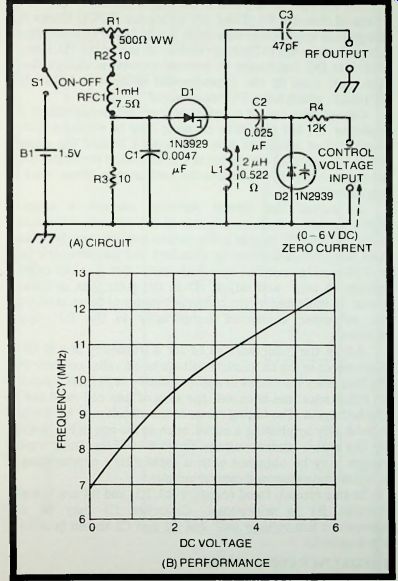
(B) PERFORMANCE
Fig. 6-4. Voltage-controlled RF oscillator.
(The unit used in the experimental setup was Miller No. 73F103AF, which has a DC resistance of 7.5 ohms.) Capacitance output coupling is provided through the 47 pF capacitor C3, but inductive coupling may be obtained with a 2-turn coil of insulated wire closewound around the ground end of L1. Any load connected to the RF output terminals must not be such that it will detune the oscillator or throw it out of oscillation.
To adjust the circuit initially, connect a suitable high-impedance frequency meter to the RF output terminals and a variable DC supply to the control voltage input terminals (this supply should either be a battery and potentiometer or a well-filtered power-line-operated unit). Set the DC control voltage to zero and adjust R1 to the point that oscillation starts, as indicated by the frequency meter or by an electronic AC voltmeter connected temporarily to the RF output terminals.
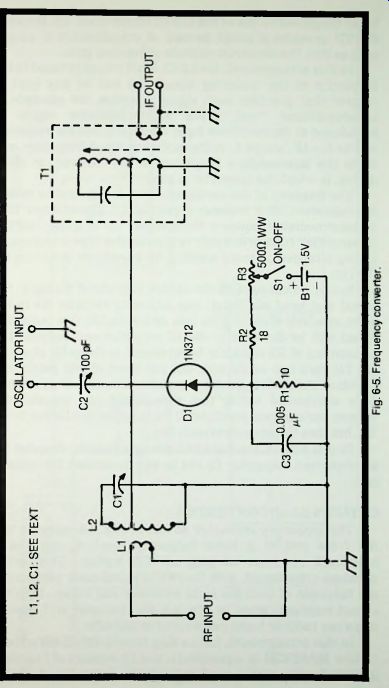
Fig. 6-5
Adjust the inductance of L1 for a frequency of 6.98 MHz.
Then increase the DC control voltage to +6 volts, and note that the frequency increases to approximately 12.58 MHz. Once the L1 inductance has been set, the slug of this coil need not be touched again. The tuning range of the circuit may be checked individually by plotting a curve, such as the one in Fig. 6-4(B), for the entire control-voltage range 0-6 volts. Other tuning ranges may be obtained with a satisfactory combination of inductor, varactor, and control voltage.
In this circuit, fixed resistors R2, R3, and R4 are 1/2-watt; rheostat R1 is wirewound. Capacitor C1 may be any convenient low-voltage unit, but C2 and C3 should be stable, low-loss units.
FREQUENCY CONVERTER
Figure 6-5 shows the circuit of a simple converter (mixer) for use in receivers and test instruments. It is conventional, but is simplified by use of the 1N3712 tunnel diode, D1. Because the TD provides a small amount of amplification in circuit such as this, the converter exhibits conversion gain.
In this arrangement, the L2-C1 input circuit is tuned to the frequency of the incoming signal and will be any type of coupler that provides such signal selection, for example, a broadcast-band "coil." The local oscillator signal is introduced at the oscillator input terminals, and its frequency will be ft -IF, where fi is the incoming-signal frequency, and IF is the intermediate frequency of the receiver, or other device, in which the converter is used.
The intensity of the oscillator signal is adjusted by means of a miniature 100 F trimmer capacitor, C2. Transformer T1 is an intermediate-frequency transformer for coupling into the IF amplifier (this preferably is a transistor-type transformer having a tapped primary winding for impedance matching for the TD).
Initial adjustment of the circuit consists of tuning-in the signal and local oscillator, and adjusting rheostat R3 to the point at which the TD goes into operation. At this point, the signal will be detected in the IF amplifier and beyond. The adjustment of R3 must not be advanced to the point at which the TD goes into oscillation, but just short of this point; it is then that the 1N3712 provides amplification, as well as mixing.
It is worthwhile noting that this circuit can operate also without the external oscillator if R3 is set for oscillation in the TD. but then the amplification is lost.
In this circuit, the fixed resistors are 1/2-watt; rheostat R3 is wirewound. Capacitor C3 can be any convenient low-voltage unit.

Fig. 6-6
CITIZENS BAND CONVERTER
The frequency converter shown in Fig. 6-6 operates into the front end of a lower-frequency receiver, such as a broadcast receiver, to pick up CB signals. This is an autodyne-type circuit, with the 1N3714 tunnel diode performing the functions of both the local oscillator and mixer. With the circuit constants given in Fig. 6-6, the converter will operate into a car radio or home radio tuned to 1500 kHz.
In this arrangement, L1 is a slug-tuned 0.482 - 0.680 u-H coil (Miller 40A687CBI or equivalent), and L2 consists of 2 turns of insulated wire closewound around the ground end of L1.
Together, L2 and L2 (with capacitor C1) form an input coupler for the CB signal. Inductor L3 is the local-oscillator coil and is slug-tuned; its range-like that of L1-is 0.482 to 0.680 u-H (Miller No. 40A687CBI or equivalent). The IF transformer, T1, is a converter-type unit designed for 1500 kHz (Miller No. 512-WT or equivalent).
To place the converter into operation, connect it by the shortest shielded cable to the receiver tuned to 1500 kHz. Close switch S1 and adjust rheostat for oscillation of the TD, as indicated by an electronic AC voltmeter to the anode of D1. Transformer T1 must previously have been set to 1500 kHz by adjustment of its tuning slug. Tune in the desired CB signal by adjustment of the slugs in coils L1 and L3 (the antenna/ground system should be the one that normally will be used with the receiving setup), working for maximum signal in the receiver into which the converter feeds.
This is a fixed-tune, single-channel arrangement, retuning of both L1 and L3 being necessary to change CB channels.
However, with a simple switching arrangement, separate coils may be provided for a number of channels, as desired. There is also some flexibility in the selection of intermediate frequency: the 1500 kHz IF transformer will permit some variation around that frequency, to locate a quiet spot on the receiver dial.
Fixed resistors R1 and R2 are 1/4-watt; rheostat R3 is wirewound. Capacitor C3 may be any convenient low-voltage unit, but C1 and C2 should be silvered mica.
AUDIO AMPLIFIER
Figure 6-7 shows the circuit of a tunnel-diode audio amplifier employing a single 1N3712. While this is by no means a high-fidelity circuit, it provides an open-circuit voltage gain of 10 at 1000 Hz and serves to demonstrate the capability of the TD as an amplifier of the negative-resistance type. The input impedance of the circuit is approximately 200 ohms at 1000 Hz.
The maximum input-signal amplitude before pronounced output-signal distortion is approximately 10 mV rms.
The circuit is seen to resemble that of the basic TD oscillator; and in fact it will oscillate if the setting of rheostat R3 is advanced too far. To adjust the circuit, close switch S1, apply a 10 mV, 1000 Hz signal to the AF input terminals, connect an oscilloscope to the AF output terminals, and adjust
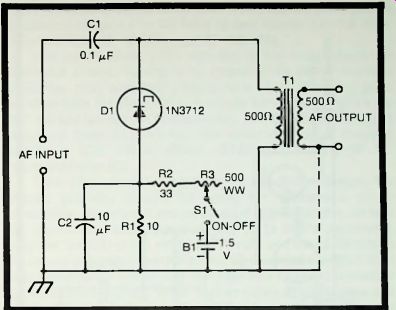
Fig. 6-7 Audio amplifier.
R3 for an output signal, as displayed by the oscilloscope. When the DC bias of the tunnel diode is incorrect for this application, the circuit will break into self-oscillation, which is usually easily identified by the fact that its frequency is different from that of the input signal. Correct bias-and highest voltage gain-is the point just below that of oscillation.
Output transformer T1 is a 1:1 unit having low DC resistance to prevent masking the negative resistance of the diode (the unit used in the experimental setup-Argonne AR-152-has a DC resistance of only 18 ohms). The fixed resistors are 1/2-watt; rheostat R3 is wirewound. Capacitor C1 may be any convenient low-voltage unit; electrolytic capacitor C2 should be a 25-volt unit.
DIP METER
The vigorous oscillation of the tunnel diode over a wide radio-frequency range, the ability of this device to operate with a 1.5-volt battery, and the small size of components associated with the TD-itself tiny-combine to make possible a dip meter that is simple and small. Figure 6-8 shows the circuit of a dip meter employing a 1N3720 tunnel diode (D1) ...
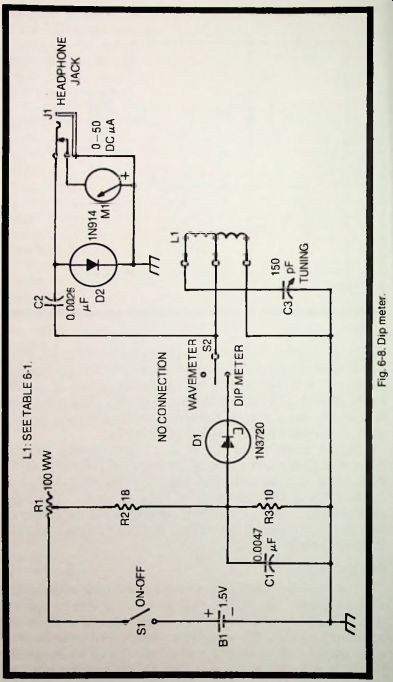
Figure 6-8
... and 1N914 conventional diode (D2). This instrument covers the frequency range 1.1 to 150 MHz in four bands: 1.1-3.8 MHz.
3.7-12.5 MHz. 12-39 MHz. and 37-150 MHz.
The tunnel diode (TD) operates in the conventional TD oscillator circuit. Tuning is by means of the 150 pF variable capacitor (C3) and four plug-in coils (L1). Table 6-1 gives winding data for these coils. A simple RF meter monitors the RF voltage across the tuned circuit, and dips when energy is absorbed from this circuit. This meter consists of coupling capacitor C2. 1N914 silicon diode D2, and 0-50 DC microammeter M1.
Following standard practice in dip meter design, the circuit provides means for using the instrument as an absorption wavemeter and as an aural signal monitor, as well as dip meter. Thus, when switch S2 is in its wavemeter position, the TD is cut out of the circuit, and the L1-C3 circuit functions as a wavemeter with Ml as the indicator. With S2 in this position, the instrument also functions as an aural monitor of modulated signals when high-resistance headphones are plugged into jack JI (insertion of the phone plug into this jack automatically disconnects the microammeter from the circuit). When switch S2 is in its dip meter position and headphones are plugged into jack JI, the instrument functions as a heterodyne frequency meter or CW monitor, with the oscillating TD beating the signal picked up by L1.
In this circuit, both fixed resistors are 1/2-watt. Capacitors C1 and C2 are mica. Rheostat R1 is wirewound. Jack JI is a closed-circuit unit, its contacts opening automatically when the phone plug is inserted.
------------
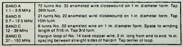
Table 6-1. Coil-Winding Data For Dip Meter BANDA 1.1-3.8 MHz BANDB 3 7-12.5 MHz BANDC 12-39 MHz BANDD 37-150 MHz 72 turns No 32 enameled wire closewound on 1 In diameter form. Tap 36th turn 21 turns No 22 enameled wire closewound on 1 in diameter form Tap 10th turn.
6 turns No. 22 enameled wire on 1 In. diameter form. Space to winding length of 7/16 in. Tap 3rd turn.
Hairpin loop of No. 14 bare copper wire. 2 in. long from end to end. Vt in. spacing between straight sides of hairpin. Tap center of loop.
-------------------
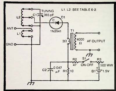
Fig. 6-9. Regenerative receiver.
The dip meter may be calibrated in any one of the conventional ways. One of the most often used methods is to couple an unmodulated RF signal source to L1, set the source to a number of selected frequencies, insert headphones, throw S2 to dip meter, and tune-in each signal by the zero-beat method. The corresponding frequency then is inscribed on the dial of C3.
REGENERATIVE RECEIVER
The regenerative receiver has a simple circuit, is relatively easy to build and use. and is a quickly assembled emergency device. An all-wave receiver of this type has already been described in Section 2. but a somewhat simpler version-employing a 1N2941 tunnel diode (DD-is presented in Fig. 6-9. This TD circuit requires only a 1.5-volt battery and is capable of extreme miniaturization.
Employing a 365 pF variable capacitor (C1) for tuning, this receiver covers the frequency range 440 kHz to 30 MHz in five bands: 440-1200 kHz, 1-3.5 MHz, 3.4-9 MHz, 8-20 MHz, and 18-30 MHz. Table 6-2 gives winding instructions for the five plug-in coils that are required.
--------------
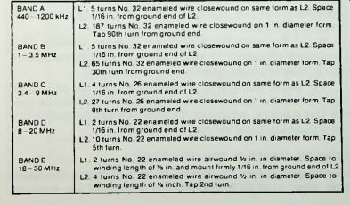
Table 6-2. Coil-Winding Data For Regenerative Receiver
BAND A 440- 1200 kHz BAND B 1-3 5 MHz BAND C 3 4-9 MHz BAND D 8-20MHZ BAND E 18-30MHZ L1 5 turns No 32 enameled wire closewound on same form as l_2 Space 1/16 in from ground end of L2 L2 187 turns No 32 enameled wire closewound on 1 in diameter form Tap 90th turn from ground end L1 5 turns No 32 enameled wire closewound on same form as L2 Space 1/16 in from ground end ol L2 L2 65 turns No 32 enameled wire closewound on 1 in diameter form Tap 30th turn from ground end L1 4 turns No 26 enameled wire closewound on same form as L2.
Space 1/16 in. from ground end of L2 l 2 27 turns No 26 enameled wire closewound on 1 in diameter form Tap 9th turn from ground end L1 2 turns No 22 enameled wire closewound on same form as L2. Space 1/16 in. from ground end of L2 L2 10 turns No 22 enameled wire closewound on 1 in. diameter form Tap 5th turn.
L1 2 turns No 22 enameled wire air-wound 'Z? in. in diameter Space to winding length of '/b in. and mount firmly 1/16 in from ground end of L2 L2 4 turns No 22 enameled wire air-wound 1/2 in. in diameter Space to winding length of V* inch. Tap 2nd turn
----------------
The circuit is basically that of a TD oscillator. The tunnel diode is a tapped down coil L1 for better impedance match and minimum broadening of the tuning. Rheostat R3 can be used to some extent as a regeneration control by using it to adjust operation of the circuit to a point just short of oscillation. The non-oscillating state is desired for reception of modulated signals, while the oscillating state must be used for CW reception.
Audio output is coupled from the detector by a miniature 3:4000-ohm transformer, T1. The DC resistance of the primary winding of this unit must be very low-otherwise it will mask the negative resistance of the tunnel diode (the transformer used in the experimental setup, Argonne AR-125, has a DC resistance of only 14 ohms). The secondary of the transformer can feed high-resistance headphones or an audio amplifier.
The receiver can be calibrated in the conventional manner, with a signal generator connected to the antenna and ground terminals, and the dial of tuning capacitor C1 marked off according to selected generator frequencies. Either modulated or CW signals may be used.
In this circuit, the two fixed resistors are Va-watt; rheostat R3 is wirewound. Capacitor C2 may be any convenient low-voltage unit.
FLEA-POWERED CW TRANSMITTER
Figure 6-10 shows the circuit of a very low-power CW transmitter employing a 1N3720 tunnel diode. In spite of its low power (approximately 1.3 milliwatts DC input), this little transmitter can perform surprisingly well when connected to a good outside antenna and operated on a clear channel.
Fig. 6-10. Flea-powered CW transmitter.
The circuit is that of the basic self-excited TD radio-frequency oscillator. The diode is tapped down tuning coil L1 for improved impedance match. Rheostat R1 is adjusted to the point that the TD oscillates vigorously, as indicated by an RF voltmeter connected temporarily to the RF Output terminals or by a CW receiver coupled to L1 or connected to the RF Output terminals. For the amateur bands, commercial plug-in coils are available for L1 and L2; these should be the center-tapped, end-link type, designed for 50 pF tuning capacitance.
Fixed resistors R2 and R3 are 1/4-watt; rheostat R1 is wirewound. Capacitor C1 should be mica. All construction and wiring must be solid to guarantee a steady signal.
For better stability than that provided by the self-excited oscillator, the crystal oscillator shown in Fig. 6-3 can be used.
For this purpose, substitute the telegraph key for switch S1 in the crystal-oscillator circuit.
REMOTE-CONTROL TRANSMITTER
Figure 6-11 shows a remote-control transmitter that can be built small enough to conceal in the palm of the hand and which can be used for working radio-controlled models, garage-door openers, and similar devices. This unit is a 27.255 MHz crystal oscillator employing a 1N3716 tunnel diode. A detachable whip antenna (this can be a 1 foot length of stiff copper wire) radiates the control signal when pushbutton switch S1 is depressed. Alternatively, the antenna can consist of several turns of insulated hookup wire wound around the inside of the nonmetallic case of the controller.
The oscillator is tuned to crystal frequency by adjusting the slug in the 0.265-0.330 u-H coil, L1. This coil must have very low DC resistance, to prevent masking the negative resistance of the diode (the coil used in the experimental model. Miller No. 40A337CBI, has a DC resistance of only 0.029 ohm).
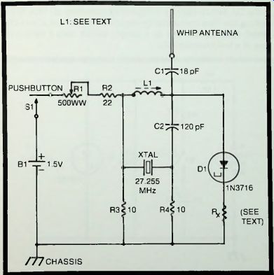
Fig. 6-11. Remote-control transmitter.
To adjust the circuit initially, depress S1 and work alternately between the settings of R1 and L1 until the circuit oscillates vigorously, as indicated by a CW monitor (see Section 5) or receiver. When R1 is correctly adjusted, oscillation will occur readily each time S1 is depressed.
When desired, the oscillator may be amplitude modulated by applying the audio modulating signal to resistor Rx, shown dotted in series with the diode. This resistance will range between 1 and 4.7 ohms, depending upon the available audio power and the characteristics of an individual TD.
TRIGGERED SWITCH
The tunnel diode exhibits two stable states, lying on opposite sides of the negative-resistance region. These stable states lie in the region OA and the region BC in Fig. 6-1(0. If the diode is biased normally in the OA region, then a momentary increase in this bias will switch operation to the BC region, and the diode will continue to operate here even after the bias is reduced to normal. Operation may be returned to the OA region only by temporarily removing all bias or by making the bias momentarily negative. This action allows the tunnel diode to function as a simple switch with a switching time of a few nanoseconds.
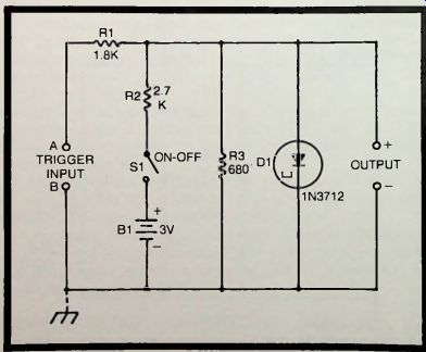
Fig. 6-12. Triggered switch.
Figure 6-12 shows the circuit of a tunnel-diode switching circuit employing a 1N3712 unit. The voltage divider, R1-R2, initially biases the TD to its low-voltage state, and the voltage at the output terminals is approximately 55 mV. Then, when a fast. 2-volt pulse is applied at the trigger input terminals to make A positive and B negative, the circuit switches rapidly to its high-voltage state, and the voltage at the output terminals increases to approximately 250 mV. The output voltage remains at this level until a 2-volt negative pulse is applied to the trigger input terminals, whereupon the output voltage is switched back to 55 mV.
An electronic switch of this type has many applications in switching and control systems, logic devices, and memories, where its simplicity recommends it.
In this circuit, all three resistors are 1/2-watt. All wiring should be kept as well separated as practicable to prevent pickup and coupling of interference via capacitance between leads.