The variable-capacitance diode (VCD) is a junction diode that has been specially processed to make useful the inherent voltage-variable capacitance of reverse-biased PN junctions. The VCD therefore can act as a tiny DC voltage-tuned capacitor in various electronic circuits, such as LC tuners and automatic frequency control systems.
All reverse-biased semiconductor diodes exhibit voltage variable capacitance, but this capacitance is very small in conventional diodes. In the VCD. capacitance is provided in useful amounts. The VCD is also called a varactor or a voltage-variable-capacitance diode (VVCD). It is also known by several trade names, such as Epicap, Semicap, and Varicap.
Because the VCD junction is reverse biased, it draws very little current (in some instances less than 1 nano-ampere) from the DC control-voltage source, and therefore is to all practical purposes a voltage-controlled--i.e.. "zero voltage''-device. Increasing the control voltage to its nominal value (as given by the VCD manufacturer) will decrease the capacitance to one-half its initial (zero-voltage) value. Up to a 10:1 capacitance change is readily obtainable at voltages higher than nominal, however. Depending upon make and model, the Q of a variable-capacitance diode is several hundred at frequencies of several hundred megahertz. Figure 7-1 shows the circuit symbol of the VCD.
Fig. 7-1. VCD circuit symbol.
Before working with VCDs, read the hints and precautions in Section 1.
VCD THEORY
The variable-capacitance diode contains an abrupt PN junction. In every junction, there is a depletion layer about the junction, that is. a region in which no current carriers (or. at least, only a trace of them) are present. This layer thus is equivalent to a thin dielectric. The N- and P-regions, which are good conductors, face each other on opposite sides of the depletion layer and act as the two plates of a capacitor with the depletion layer acting as the dielectric of this capacitor.
When no external voltage is applied to the diode, the depletion layer is thin and the junction capacitance is highest (see Fig. 7-2A). But when a reverse DC voltage is applied to the diode (that is. anode negative and cathode positive), the depletion layer widens by an amount proportional to the voltage, and the capacitance decreases (see Fig. 7-2B). It is in this way that a variable DC voltage makes the diode a variable capacitor. The junction being reverse biased, any direct current flowing through the diode from the control-voltage source is minute (usually in the nano-amperes), so virtually no power is required to tune this semiconductor capacitor.
Figure 7-2 (C) shows typical performance of the VCD. From this plot, notice that an increase in voltage from zero to ll2 times the nominal value decreases the capacitance from approximately 260% of nominal capacitance value to approximately 80% of nominal capacitance. This means that a VCD rated at 100 pF at 4 volts would show a capacitance change from 260 pF at zero volts to 80 pF at 6 volts. Common nominal capacitance values for VCDs are given in steps from 6.8 pF to 100 pF. although values of several hundred picofarads ...
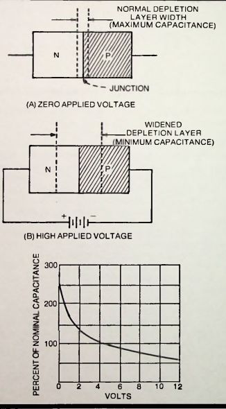
Fig. 7-2. VCD action.
... are sometimes manufactured. A common nominal voltage is 4 VDC. and maximum permissible voltages are given in steps from 15 VDC to 150 VDC.
VOLTAGE-VARIABLE CAPACITOR
When an adjustable DC voltage is available from any source, it can be used to vary the capacitance of a variable-capacitance diode, and a DC-tuned miniature variable capacitor results. Such a component has a great many applications in communications and general electronics.
Any VCD may be employed in this manner, the unit chosen being selected for desired voltage and capacitance ratings.
Figure 7-3 (A) shows the circuit of a voltage-variable capacitor offering a 4.1 capacitance range. The capacitance seen at the capacitance terminals varies from approximately 260 pF to 65 pF as the DC control voltage varies from zero to 4-12 volts. Figure 7-3(B) details this performance.
In this circuit, the 1-megohm, 0.5-watt resistor (R1) isolates AC energy applied to the capacitance terminals in applications in which the voltage-variable capacitor is used, keeping it out of the DC voltage source. This resistor replaces the usual choke coil in this function; and since the VCD draws virtually no current in its reverse-biased condition, there is practically no voltage drop across R1.
The 0.01 u-F capacitor (C1) protects the V100EB variable-capacitance diode (D1) from any DC component in the external circuit in which this arrangement is used. Since the capacitance of C1 is large, with respect to that of diode D1, the capacitance seen at the capacitance terminals is principally that of the diode. The V100EB diode is rated to withstand a maximum bias of 10 VDC, and at this voltage the reverse leakage current is only 100 nano-amperes.
The AC voltage presented to the capacitance terminals must be small, with respect to the DC control voltage; otherwise the AC voltage, instead of the DC. will determine the diode capacitance. In most instances, this will occasion little difficulty, since the signal voltage will ordinarily be small, compared with the 1 to 12 volts for control voltage.
Several VCDs may be connected in parallel to increase the maximum obtainable capacitance. It must be remembered however, that the parallel connection will also increase the minimum capacitance. Thus, five type V100EB units connected in parallel in the circuit of Fig. 7-3 (A) will provide a maximum capacitance (zero VDC) of approximately 1300 pF, and a minimum capacitance (12 VDC) of approximately 325 pF.
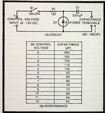
Fig. 7-3. Voltage-variable capacitor.
In short, all of the capacitance values in Fig. 7-3 (B) will be multiplied by 5. At the same time, the leakage current will be 1/5 of the rated value for a single VCD (in this case 20 nano-amperes).
The electronic-type variable capacitor is smaller than the tiniest manually variable capacitor of the same capacitance.
Obviously, if a potentiometer is used to vary the capacitance-controlling DC voltage, this potentiometer may well be as large as-or even larger than-an equivalent plate-type capacitor; however, this may be of no moment when the electronic capacitor is to be remotely controlled. In many applications, the variable DC voltage will already be available in a circuit in which the electronic capacitor is used.
VCD-TUNED LC CIRCUITS
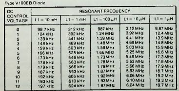
Table 7-1. VCD-Tuned Circuit Data
Figure 7-4 shows several circuits in which the voltage-variable-capacitance of a VCD is employed to tune an inductance-capacitance (LC) circuit. In these examples, a type V100EB diode is shown. The capacitance of this unit varies from 260 pF when the DC control voltage is zero, to 65 pF when the voltage is 12 (see Fig. 7-3B). Table 7-1 shows the resonant frequencies corresponding to the DC control-voltage value (in steps of 1 volt from zero to 12 volts) for five different values of inductance, L1.
Figure 7-4 (A) is the basic circuit, which is used as is in most applications of VCDs. Here, capacitor C1 prevents short circuit of the DC control voltage by inductor L1. This capacitance is so large, with respect to that of the VCD, that the VCD rather than C1 tunes the inductor. Resistor R1 acts somewhat as an RF choke, blocking the AC signal in the tuned circuit from the DC supply.
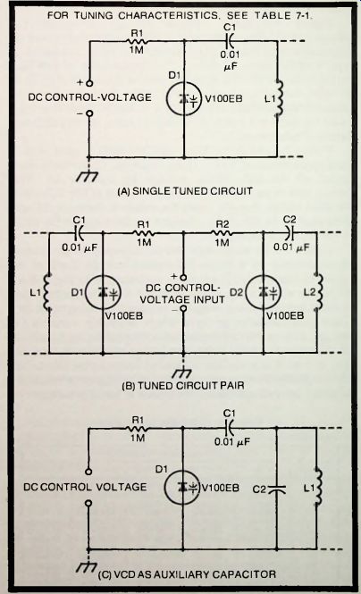
Fig. 7-4. VCD-tuned LC circuits.
Figure 7-4 (B) shows how two circuits may be gang-tuned simultaneously by a single DC control voltage. Each of the halves in this circuit is identical with the one in Fig. 7-4(A). While two circuits are shown in Fig. 7-4(B), the method may be extended to as many stages as required, all being tuned by a single potentiometer or by a single available variable DC voltage. Figure 7-4(0 contains an additional tuning capacitor, C2. Whereas the VCD is the lone tuning capacitor in 7-4A and (B), in 7-4C it is a voltage-controlled trimmer for fine-tuning the frequency in response to a DC error signal or manually adjusted DC voltage. Here, the circuit is tuned principally by means of conventional variable capacitor C2. The capacitance of the diode is effectively in parallel with C2 and therefore can retune the circuit above and below the point established by the setting of C2. In practice, the diode capacitance is chosen considerably lower than that of capacitor C2, thus insuring that C2 is the dominant frequency-determining capacitance.
The circuits in Fig. 7-4. and logical modifications of them, find use in receivers, transmitters, instruments, and control devices. When the scheme in Fig. 7-4(B) is extended to several stages, a small voltage-controlling potentiometer can take the place of a bulky multi-gang tuning capacitor. Because of the low capacitance of VCDs, these circuits are usually limited to radio frequencies. However, it is possible to parallel connect two or more VCDs for higher capacitance.
While the V100EB diode is shown here as a practical example, other VCDs may be selected for particular applications.
REMOTELY CONTROLLED TUNED CIRCUIT
One of the obvious applications of the DC tuning of an LC circuit is the tuning of a distant device, such as a receiver or instrument. This technique has been used, for example, to tune a field-strength meter located out of the near zone of an antenna under test, the output current from the instrument being sent back by cable to the test shack to operate an indicating meter. It has been used also to tune a distant transmitter.
Figure 7-5 shows an example of this application. In this arrangement, the DC control voltage is transmitted through a shielded cable to the voltage-variable capacitor (D1) at the remote location. This voltage is adjustable from zero to 12 volts by means of a 10.000-ohm wirewound potentiometer (R1). The V9000EB diode shown here has a capacitance of approximately 260 pF at zero VDC and 65 pF at 12 volts, and is a low-leakage type (5 nA at 20 volts), but other VDCs may be employed, as desired.
The 470 K resistors (R2 and R3) and the associated 0.001 uF capacitors ( C1 and C2) effectively block the AC signal associated with the L1 tuned circuit from the DC supply. The 0.01 u-F capacitance of C3 is so large with respect to that of the diode that the latter, rather than C3, tunes inductor L1. The inductance of L1 is governed by the frequency of the device in which this remotely tuned circuit operates.
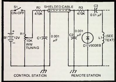
Fig. 7-5. Remotely controlled tuned circuit.
Table 7-1 lists five common inductor values and shows the frequencies corresponding to control voltages between zero and 12 volts for each of these inductances. The dial of potentiometer R1 may be graduated in kHz or MHz on the basis of an initial calibration of the circuit. Although a continuously variable DC control voltage is at work in the circuit as shown in Fig. 7-5, the control voltage may instead be applied in discrete steps for step-tuning of the resonant circuit.
VOLTAGE-TUNED RF OSCILLATOR
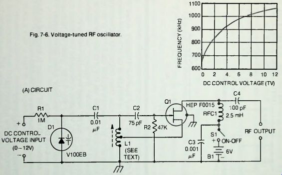
Figure 7-6.
Figure 7-6 shows how a VCD can be used to DC voltage-tune a radio-frequency oscillator. Figure 7-6(A) gives the circuit, and Fig. 7-6(B) the tuning performance. The oscillator is a tapped-coil Hartley circuit employing a type HEP FOO 15 field-effect transistor ( Q1), but any similar circuit can also be used. The oscillator tank coil (L1) is tuned by the type V1000EB variable-capacitance diode (D1), which is connected across the coil through 0.01 u-F capacitor C1. (The capacitance of C1 is so high, with respect to that of the VCD that the latter rather than C1 tunes the coil.) For the 600-1078 kHz range (see Fig. 7-6B), L1 must be a slug-adjusted 0.04-0.24 mH coil with a tap at 1/3 of its turns (J. W. Miller No. 9011, or equivalent).
Figure 7-6(B) shows how the frequency varies from approximately 645 kHz to 1078 kHz as the DC control voltage is varied from zero to 12 volts. Other frequencies and ranges may be covered by substituting a suitable coil for L1. In the initial adjustment of the oscillator, the slug of L1 is set for 645 kHz (as indicated by a suitable frequency meter connected temporarily to the RF output terminals) with the DC control voltage set to zero. Variation of the control voltage then should reproduce the curve of Fig. 7-6(B), within the tolerance of individual VCDs. The oscillator draws approximately 5 mA from the 6-volt DC supply.
Another VCD-tuned RF oscillator is described in Section 6, that one being based on a tunnel-diode oscillator.
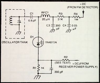
Fig. 7-7. Automatic frequency control for FM receive.
AUTOMATIC FREQUENCY CONTROL FOR FM RECEIVER
The DC output of an FM detector may be used as an error voltage to vary the capacitance of a VCD which, in turn, will automatically reset the tuning of the front end. The basic circuit for accomplishing this action is shown in Fig. 7-7. In principle, this is the same arrangement used with tubes or transistors for automatic frequency control (AFC). As shown here, the VCD acts as a trimmer in the front-end oscillator tank (see Fig. 7-4C and the attendant discussion for a description of the VCD as a trimmer), and capacitor C1 prevents the oscillator coil from short-circuiting the DC control voltage. The 1N4815A variable-capacitance diode is rated at 100 pF at 4 VDC.
The operating point of the diode is 5 volts provided by the DC power supply of the receiver through voltage divider R1-R2. Resistor R1 must be 1000 ohms, but R2 will depend upon the power-supply voltage, and the correct resistance may be calculated:
R2 = (200 Es) - 1000
... where R2 is in ohms and Es in volts.
Thus, for a 35-volt supply, R2 = (200 X 35) - 1000 = 7000 - 1000 = 6000ohms.
The DC voltage must be well regulated; otherwise, the diode capacitance will fluctuate with the voltage (and so will the receiver tuning). The FM detector has no DC output, as long as the receiver is tuned sharply to a station. On detuning, however, a proportional DC voltage is delivered by the detector, and it is this voltage acting on the VCD that retunes the receiver to the station.
To compensate for the presence of the AFC circuit in the oscillator, the receiver must be carefully realigned after the AFC circuit has been installed. For an individual VCD. it may be necessary to adjust R2 critically around the calculated value, for optimum AFC action. Since the VCD draws virtually no DC. its presence will have no effect on the FM detector. A substantial RF filter (RFC1-R3-R4-C3-C4 in the detector output line) provides essential RF isolation.
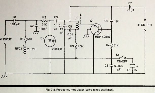
Fig. 7-8
FREQUENCY MODULATORS
When a VCD is used as a frequency-varying device in a radio-frequency oscillator, modulation of the VCD capacitance will frequency modulate the oscillator. This provides a simple way of obtaining an FM signal either in a transmitter or in a signal generator.
In most applications, an audio modulating voltage is applied to the VCD which is DC biased to a point along its voltage/capacitance curve that affords linear operation. The radio frequency then varies at the audio rate, and the deviation is proportional to the peak audio-voltage swing. By adjusting the audio amplitude, the operator may easily obtain either narrow-band or wideband FM, as desired.
Figure 7-8 shows how an audio-modulated VCD may be employed to frequency modulate a self-excited oscillator. The oscillator is a tapped-coil Hartley arrangement using a HEP S0016 bipolar transistor (Q1). For this type of oscillator, the tank coil (L1) must be tapped one-third of the way from the ground end. and such a tap is normally provided in the commercial coil (Miller No. 9012) used in the author's circuit.
The oscillator is tuned principally by coil L1 and capacitor C4; the variable-capacitance diode (D1) serves as a DC-variable trimmer, and is biased by the same 9-volt battery that energizes the transistor. The RF filter (RFC1-R-R2-C2) isolates the DC supply with respect to RF, and the series capacitor (C3) prevents coil L1 from short-circuiting the DC.
The tuned circuit of the oscillator has been chosen for 1000 kHz operation, but operation may be obtained at any other carrier frequency by suitably choosing the L1 or C4 values.
(The higher the carrier frequency, the greater will be the FM swing per audio volt.) For initial adjustment of the circuit, slug-tone coil L1 for the carrier frequency with zero audio volts at the AF input terminals. Then apply the audio modulating voltage, and note the FM deviation for various audio amplitudes.
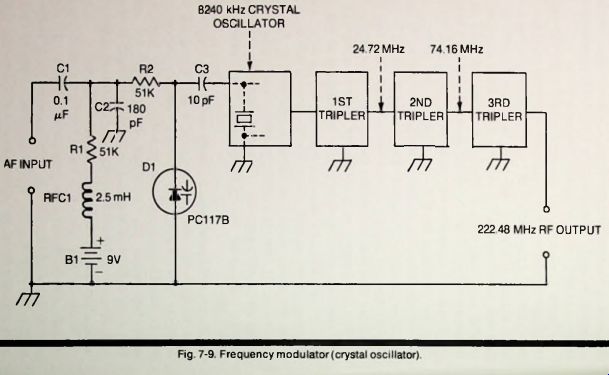
Figure 7-9
Figure 7-9 shows how an audio-modulated VCD may be used to fluctuate the frequency of a quartz crystal in an oscillator stage and so to frequency modulate the oscillator.
The crystal frequency can be varied only a few hertz in this way. but when the oscillator is followed by several frequency-multiplier stages, this variation is multiplied along with the carrier frequency, and a useful amount of frequency modulation may be obtained in the output stage.
Thus, in Fig. 7-9. the oscillator is followed by three triplers. and here a crystal-frequency variation fluctuation of only 100 Hz would result in a fluctuation of 2.7 kHz at the final output. The circuit given here is designed to operate in the 220 MHz amateur band, the final output based upon the 8240 kHz crystal being 222.48 Mhz. Varactor-type (i.e., VCD type) triplers are described in the following sections.
In this arrangement, a type PC117B, high-Q, variable-capacitance diode (DI) operates in parallel with the crystal through DC-blocking capacitor C3. Audio modulating voltage is applied to the VCD against the operating-point-setting DC bias provided by DC source B1 through the RF filter RFC1-R1-R2-C2. The resulting variation of the VCD capacitance at the audio rate fluctuates the frequency of the crystal. The deviation of the crystal frequency is proportional to the audio amplitude, and this deviation is multiplied successively by the triplers.
While the scheme shown here utilizes a 8240 kHz crystal to obtain frequency-modulated operation at 22.48 MHz, the same general arrangement may be applied for other output frequencies by suitably choosing crystal frequency and the number and type of multipliers. (The higher the final carrier frequency, the greater will be the FM swing per audio volt.) In both the self-excited and the crystal circuit, some experimentation with the DC operating point of the VCD is necessary in order to obtain the most linear modulation. The purpose of this bias, in each circuit, is to set the operating point of the VCD to the most linear part of the diode voltage vs-capacitance characteristic.
VCD-type frequency modulators, whether employed with self-excited or crystal oscillators offer the advantages of simplicity and ease of adjustment. Moreover, the VCD requires no audio power for its operation, so the modulating source can be simply a voltage amplifier. The VCD modulator may easily be built into an existing oscillator and will occasion only the slightest readjustment of the oscillator alignment or tuning.
It is informative to note the frequencies at which FM is authorized in the ham bands. For wide-band FM: 29-29.7, 52.5-54. 144.1-148. 220-225. and 420-450 MHz. For narrow-band FM: 3775-4000 kHz. 7150-7300 kHz, 14.2-14.35, 21.25-21.45.28.5-29.7. and 50.1-54 MHz.
FREQUENCY MULTIPLIERS
It is clear in the capacitance/voltage characteristic curve of the VCD (Fig. 7-2C) that a considerable portion of the operation of this device is nonlinear. Because of this nonlinearity, the VCD can distort an alternating current flowing through it. and accordingly can act as a harmonic generator. Indeed, the attractiveness of the VCD as a harmonic generator is now well exploited in frequency doublers and triplers.
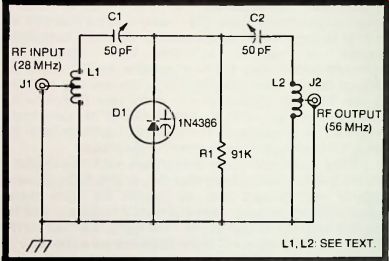
Fig. 7-10. Frequency doubler.
In this application, in which the VCD is called a varactor, no DC supply is needed, so the frequency multiplier is both simple and economical. Furthermore, it is efficient (90% is typical for varactor-type doublers, compared with 50% for the tube-type), since the VCD-a reactive device-draws very little power from its driving source. Figure 7-10 shows one type of varactor doubler, and Fig. 7-11 a varactor tripler.
In the doubler. Fig. 7-10, the input circuit is tuned to the frequency of the driver, and the output circuit to twice that frequency. In this instance, inductor L1 and capacitor C1 are tuned to 28 MHz. and inductor L2 and capacitor C2 to 56 MHz.
For these frequencies, the coils have the following specifications:
L1-7 turns No. 14 enameled wire air-wound 1 in. in diameter.
Space to winding length of 1 inch. Tap 2 1.5 turns from ground end.
L2-5 turns No. 14 enameled wire air-wound 1 in. in diameter.
Space to winding length of 1.25 inch. Tap second turn from ground end. Other capacitor and inductor combinations may be employed for desired input and output frequencies. A 1N4386,50-watt. varactor (D1) is used in this circuit.
In the tripler-Fig. 7-11, the input circuit is tuned to the frequency of the driver, an idler circuit to twice that frequency, and the output circuit to three times the driver frequency. The purpose of the idler (L3-C2) is to reinforce the tripler action and increase the overall efficiency of the circuit.
In this instance, inductor L2 and capacitor C1 are tuned to 74 MHz, inductor L3 and capacitor C2 to 148 MHz, and inductor L4 and capacitor C3 to 222 MHz. The coil specifications for these frequencies are given in Table 7-2.
Other capacitor and inductor combinations may be employed for desired input and output frequencies. A 1N4386, 50-watt, varactor (D1) is used in this circuit.
Varactor doublers and triplers can be operated in cascade in various combinations to obtain desired output frequencies from available driver frequencies. While doublers and triplers are usual in varactor multiplier stages, frequency quadrupler action also has been reported.
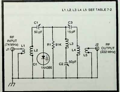
Fig. 7-11. Frequency tripler.
----------

Table 7-2. Coil-Winding Data For Frequency Tripier L1 3 turns No. 22 enameled
wire closewound on same form as L2. Space Vb in. from ground end of L2.
L2. 35 turns No. 22 enameled wire closewound on 1 in. diameter form.
L3.16 turns No. 14 enameled wire air-wound 1 in. in diameter Space to winding length of 114 inch.
L4.3 turns No. 14 enameled wire air-wound 1 in. in diameter. Space to winding length of 1 inch.
L5.1 turn No 14 enameled wire solidly mounted '/a in. from ground end of L4.
---------
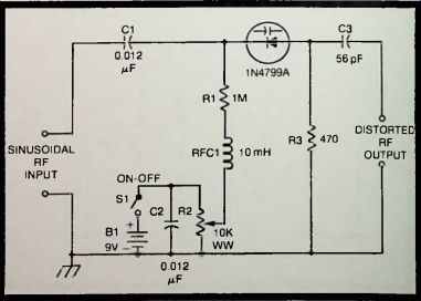
Fig. 7-12. RF harmonic intensifier.
RF HARMONIC INTENSIFIER
The nonlinearity of the VCD, so useful in frequency multipliers, can be enlisted to accentuate the harmonics of a signal source, such as a frequency standard. The very high-order harmonics from such a source are often too weak to be useful, and can be brought up to useful amplitude by means of a simple, untuned intensifier circuit.
Figure 7-12 shows the circuit of a harmonic intensifier designed primarily for use with a 100 kHz crystal oscillator used as a secondary frequency standard band-spotter. In this arrangement, a 1N4799A diode is biased by means of the DC circuit (B1-R2) to the most nonlinear point in the diode capacitance/voltage characteristic, as evidenced by the strongest harmonic output. The RF input-signal current flowing through the VCD and resistor R3 in series then is distorted by this nonlinear response. The output voltage, developed across resistor R3. accordingly contains a high percentage of harmonics. The intensifier circuit produces negligible loading of the signal source.
Use of the circuit is straightforward: Close switch S1 and adjust potentiometer R2 for the strongest signal, as heard in the receiver, monitor, frequency meter, or other device with which the signal source is used. The proper setting of R2 can mean, for example, hearing or not hearing the 15 MHz harmonic of a 100 kHz oscillator.
The intensifier can be built into a small case. Battery drain is 0.9 mA DC.