AMAZON multi-meters discounts AMAZON oscilloscope discounts
Power transistors make effective switching devices for power conversion from either DC to DC, DC to AC, or AC to DC. Transistors are more reliable than vibrators, and are not as complex or bulky as motor-generators. Also, their efficiency is very high.
High-voltage, low-current DC is used for mobile-radio plate supplies, and low-voltage, high-current AC is applied to servo systems and AC motors. Power conversion from low- to high voltage DC requires a DC-to-DC converter, while conversion from low-voltage DC to AC requires an inverter. By adding a rectifier filter to an inverter, a DC-to-DC converter can be produced.
700-WATT INVERTER
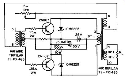
----------- 700-watt inverter.
This circuit shows a two-transistor inverter using 2Nll67 power triodes, which have a current gain of 25 at 25 amperes and can thus switch 700 watts ( 25 amperes at 28 volts). A 10-CFM blower is used to stabilize the case temperature to below 60°C. The transistors are insulated from the heat sink with an anodized aluminum washer, and silicone grease helps lower the thermal resistance from the transistor case to the heat sink.
The two-transformer design allows the feedback transformer to do the saturating while reducing the collector-current spikes.
Since the output transformer does not saturate, saturation losses are reduced considerably. The driver transformer is designed to oscillate from 200 to 1,200 cycles with a 2- to 12-volt drive. A multiple tap on the output transformer is wound onto a double 4½-inch Hypersil C core, each half having a cross section of about ¾ inch. The driver transformer consists of three identical windings of No. 16 trifilar-wound wire to provide various circuit configurations. The driver core is laminated of mu-metal with a core area of about 3/s square inch and about 1 " x 1 " x ½" outside dimensions. The circuit is operated common-emitter push-pull. A 0.5-ohm potentiometer is inserted between the feedback winding and driver transformer to allow proper switching and to help control the frequency. Performance is improved by inserting 0.25-ohm resistors in series with the base to equalize the drive and eliminate burnout.
From this circuit a power output of 575 watts is obtained with a power input of 700 watts, for a loss of 125 watts and an efficiency of about 82 % . Bias and feedback resistors account for about 25 watts, while another 35 watts is lost in the transistors.
The remaining 65 watts apparently is lost in the transformers.
An additional 20 watts is required to operate the blower, which is driven from the output. Currents of up to 34 amperes can be switched and power outputs of more than 700 watts obtained intermittently.
FIELD-EFFECT TRANSISTOR IMPEDANCE CONVERTER
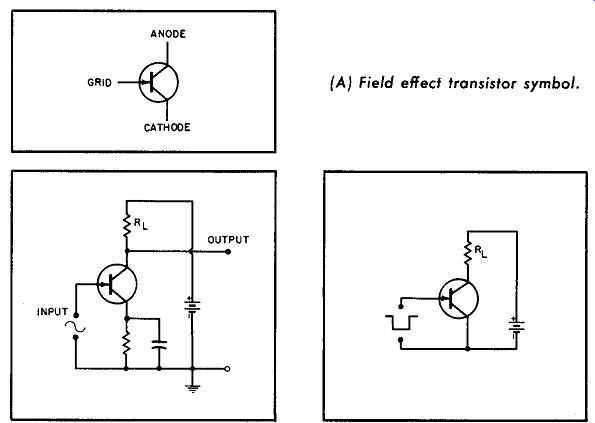
----------- Field effect transistor-impedance converter. (A) Field effect
transistor symbol. (B)High input impedance amplifier and converter.(C) Switching
circuit.
The noise parameters of the field-effect transistor in Part A will be extremely low-even with a very high source impedance provided the anode voltage is maintained at approximately +3 volts. The device then operates in the triode region and hence is extremely useful as the input stage in very low-noise, high impedance transistor amplifiers. The output impedance of the device in the triode region is approximately 2.5K, which is the ideal source impedance for conventional low-noise transistors following the input stage.
As in the circuit of B, R1 should be at least 10K to avoid undue loss of signal. The stage operates at about unity voltage gain.
Impedance converters can also be used as matching devices, where it is desired to use an ordinary transistor amplifier but no signal loading is permissible.
Field-effect transistors can be used as switches in digital applications, as in Part C. Unlike transistors, they require pulses of only one polarity for full on-off operation. The device is on when no voltage appears on the grid, and off when the grid is pulled negative. In the "off" condition, the resistance of the device is around 100 megohms, and the "on" resistance is approximately 2K. Since the input capacitance is approximately 50 mfd, the switching speeds are directly affected by the impedance of the generator driving the switch. For a high switching speed, the driving generator is of low impedance during both build-up and collapse of the driving pulse.
INVERTER (12VDC to 110VAC)
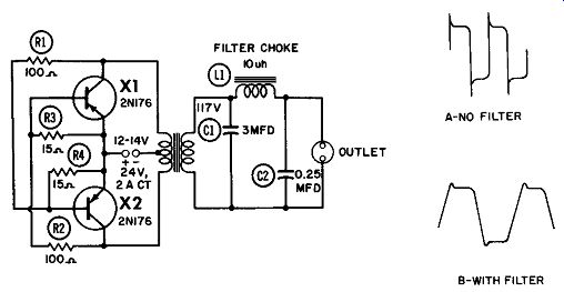
There are several forms of inverters in use. A 50-watt output at 0.5 amperes and 110 volts AC can be obtained from a pair of 2N176 power transistors connected as shown. This is enough power to operate a small phonograph, AC-DC radio, dictating machine, small soldering iron, or a trouble light. Efficiency is about 75% DC-to-AC. As shown, base bias and collector-to-base coupling are provided through 100-ohm, 2-watt resistors R1 and R2. Bias stability is provided by 15-ohm, 2-watt resistors R3 and R4.
Inverter (12VDC to 110 VAC).
This inverter, designed for use with AC equipment, has a frequency output of approximately 60 hz and a peak-to-peak voltage ( between the flat tops) of 250 volts at 50 watts. For many applications this output is satisfactory, even though the waveform is approximately a square wave without the filter. The hash filter ( composed of C1, L1, and C2) removes most of the spikes, giving a trapezoidal waveform. With the filter, the frequency is reduced to about 56 hz.
6-KV INVERTER
Inverters can provide power for several applications. An inverter for 6 to 6,000 volts AC is shown here. This 6 kv can be doubled and used for CR tubes. On the left is the inverter, which uses a pair of 2Nl76's in a common-collector circuit.
The transformer is special; the Ceramag U core, AP 11-264(2), is similar to the type often used in TV flyback transformers. L1 and L2 are hand-wound side by side on the cardboard bobbin, with taps brought out on either side. The winding is covered with three thicknesses of bond paper saturated with coil dope.
L3 is universal-wound onto this paper layer. The winding is ¾ inch wide. After every 250 turns, a layer of doped paper is applied to the winding to strengthen the coil. This builds up the winding to a diameter of approximately 2¾ inches. The coil is thoroughly doped, then dried, and covered on the sides and top with masking tape painted with dope. Each coil is wound as follows:
L1-6 turns, C.T. No. 18 Nylclad L2-10 turns, C.T. No. 18 Nylclad L3-3,500 turns, No. 36 Nylclad, Silk
-------------- 6-KV inverter.
6-KV inverter.
The inner lead of L3 is grounded to any convenient point on the frame, and the outer terminal brought out by a well-insulated lead. Windings L1 and L2 must be correctly phased in order for oscillation to be obtained. Correct phasing is best established by trial and error. Reverse the base leads if oscillation is not obtained on the first try.
This unit produces a 6-kv AC output which can be combined with the unit on the right as shown. The right-hand circuit is a time-base generator which can be used as a portable flasher for warning lights ( e.g., for construction hazards). They can also be used together.
Consider the time-base generator alone. When a 6-volt supply, a 2N35, and a 2N176 power transistor are used, it is a relaxation oscillator. Network R1- C1 is the time-constant circuit, and R2 controls the pulse duration.
With S1 open there is no output. When switch S1 is closed, capacitor starts to charge, making the base of X1 more positive than the emitter. This charging rate depends on the time constant of R1-Cl. At some critical voltage, X1 begins to conduct, followed by X2. When X2 is driven into saturation, the full battery potential is across the load. Conduction of X2 causes capacitor C1 to discharge until, at a low critical value, X1 is cut off, causing X2 to be cut off also. This action is repetitive and establishes the time base.
The frequency of the circuit shown is approximately 90 pulses per minute. Other time rates can be obtained by using different values of R1 and Cl. The frequency varies inversely with the value of R1 or C1. As the value of R2 is increased, the pulse duration is also increased. In the circuit shown, the pulse duration is approximately 10 milliseconds. If R2 were increased to 1,000 ohms, the duration would be approximately 50 milliseconds.
The time-base generator can drive a 6-volt incandescent bulb for warning purposes. Connecting A and B, as shown, allows the inverter to drive gas-tube lights.
DC-TO-AC INVERTER
Both circuits shown use four-layer diodes. The first is a high efficiency circuit with a minimum of components. The second circuit provides a margin against the effects of changes in load, load power factor, or supply voltage. Supply voltages of up to 80 volts may be used with a single four-layer diode in each side of the inverter, and higher supply voltages may be obtained by adding more diodes in series.
Part A of the diagram shows a highly efficient DC-to-AC power converter. The circuit alternately switches a fixed current, sup plied through L1, into the two halves of the primary of a center tapped transformer. The frequency is controlled by input pulses to the trigger point, with two pulses required for each cycle.
The circuit can operate at any frequency, from a few hundred cycles to more than twenty kilocycles. The DC supply voltage may be from six to several hundred volts. The power output is limited by the maximum current that can be switched into the primary. The circuit efficiency is a function of the DC supply voltage; it is about 95 % for higher supply voltages and a minimum of 75% for a 6-volt DC supply.
When 4 D1 conducts, current from the DC supply passes through the loop composed of L1, P1, 4 D1, and D. This current is limited by the impedance reflected into Pl from the transformer secondary. Point A will be at the holding voltage ( 1 to 2 volts) of 4 D1 and D1 in series. The center tap of the transformer will be at Vo, and point B will-by transformer coupling between P1 and P2-be twice this voltage, or 2 Vo.
If a negative pulse of sufficient amplitude is applied to the trigger point, 4D2 will begin to conduct. The voltage on commutating capacitor Cc, which is coupled from the transformer secondary into the two primary legs, will drive point A negative.
This will switch off 4 D1. The DC supply current will be commutated from P1 into P2.
(A) High efficiency converter.
(B)Solid-state inverter.
(C) Waveforms
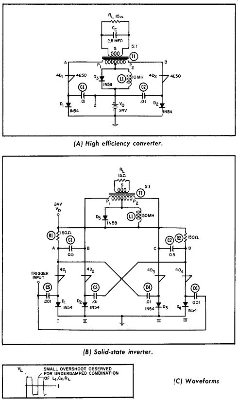
------------- DC to DC inverter.
The next negative trigger pulse will switch 4 D1 on again; and the commutating capacitor will, through transformer action, switch 4D2 off. The cycle is now completed.
The commutating capacitor must be large enough so that its voltage, when reflected into the transformer primary, is capable of turning off the diode. The commutating capacitor can be connected directly across the primary, from point A to point B. ( If located in the higher voltage secondary, a much smaller capacitor may be used.) Conventional diodes D1 and D2 must be capable of passing the high average current flowing in the circuit. For high primary currents, it is possible to replace D1 and D2 with four-layer diodes.
In high-efficiency parallel inverters, there is a tendency for both sides of the inverter to stay on when turned on. This can be prevented by using a normally closed relay in place of L1. The DC supply current passes through both the relay contacts and the actuating coil.
The solid-state inverter circuit shown in Part B protects against variations in load, load power factor, or supply voltage. The circuit is fail-safe because the supply current drops to zero when ever the load is shorted. Normal operation is resumed when the short is removed. The circuit will continue to operate normally despite large changes in supply voltage or poor load power factors.
This highly reliable circuit uses outrigger stages, which turn off the adjacent conducting legs of the basic inverter when a trigger pulse is received, independent of the state of the other basic inverter leg. The onset of conduction in an outrigger stage will also trigger the previously nonconducting inverter leg under normal operating conditions.
Design considerations for the basic inverter are the same as for Part A. Note the absence of the commutating capacitor in the transformer secondary; this function is provided by the outrigger stages.
DC-TO-DC CONVERTER (MOBILE-RADIO SUPPLY)
Transistor DC-to-DC converters are used for plate supplies because they are more efficient and reliable than other types of DC power sources. Power outputs of up to 700 watts are possible.
This figure shows a schematic of a transistor power supply designed to be added to and used with mobile radios. Two triode power transistors operating as a flip-flop oscillator are used. This oscillator is a square-wave generator with a frequency of approximately 100 to 3,500 hz.
DC to DC converter (mobile radio supply). The vibrator-type supply requires an iron-core transformer with materials and construction similar to those for 60-cycle equipment. However, the transformer in a transistorized unit weighs only a few ounces. Therefore, less filtering and shielding are needed because current switching is electronic. Square waves are a source of harmonics into the RF range, but these undesired components are not difficult to suppress.
The stepped-up voltage appearing at the transformer secondary is rectified in a bridge circuit using four silicon diodes. Ripple filtering is accomplished in a conventional RC network following the rectifiers. Power output of the transistor supply shown is usually in the 200-volt, 100-ma range, which is sufficient to power a multistage FM receiver. Over-all efficiency of the supply is 70 % to 75 % . This is the approximate efficiency of a vibrator supply using a nonsynchronous vibrator and selenium rectifier.
All components except transistors usually are mounted on a small printed-circuit board. The transistors themselves are mounted directly onto the outside of the case, which acts as a heat sink. A protective bracket covers the transistors but still permits air to circulate freely around the heat sink, which maintains the transistors within the recommended operating temperatures.
500-WATT INVERTER
This circuit is a common-emitter, grounded-collector power supply which provides 500 watts of AC output from the 28-volt DC supply. Two sets of paralleled 3N46 or 3N50 tetrode transistors are used. R2 through R5 are 3.3-ohm base resistors; R6 through R9 are 0.05-ohm emitter resistors used to equalize the collector currents.
Voltage drops across diodes D1 and D2, applied to the bases through the Thermistors, provide a bias which increases with temperature and thus prevents thermal runaway.
In operation, one pair of transistors ( X3 and X4) conducts through the lower secondary of T1 ( the DC source) and the lower half of T2. Induced current in the upper secondary of T1 switches X1-X2 on, and AC is supplied through T2 to the output.
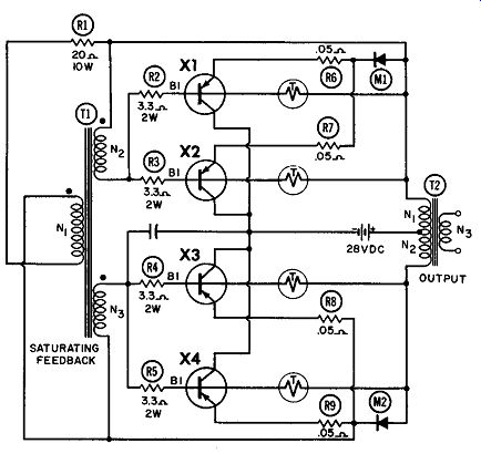
------------- 500-watt inverter.
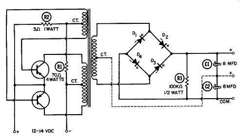
------------ 85-watt DC to DC converter.
85-WATT DC-TO-DC CONVERTER
A DC-to-DC converter using 2Nl755 transistors is shown here.
When DC-to-DC converters are operated at the higher input voltages, their transformers must be specially designed. Recommended transformer core materials are Orthonol or Deltamax with 0.002-inch laminations. Frequency of operation at approximately 2,000 hz offers best compromise between transformer size and converter efficiency, although the frequencies can be higher than 2,000 hz if the lower efficiency caused by the reduced squareness of the waveform can be tolerated. Frequency of operation is chosen and the design of the transformer primary winding calculated from the formula shown in the figure. The feedback winding provides approximately two to three volts for each base, and the secondary winding provides the proper voltage to the load. The purpose of R1 is to bleed current into the bases of X1 and X2, to promote starting at low voltage. R2, in conjunction with R1, is adjusted to provide the proper "on" base current. R2 should be from 3 to 10 ohms. The following precautions should be observed:
1. Transformer windings should be balanced and should be bifilar wound to minimize leakage reactances.
2. Switching transients in the collector-voltage waveform should be eliminated by using the "despiking" networks of a small buffer capacitor across the secondary winding.
3. The path of operation (VCE versus le) should be observed on an oscilloscope. The most reliable converters are obtained when the VcE versus le plot encloses the smallest possible area. Improvements can be made by bypassing R2 with a large capacitor and by assuring that the "on" base current does not exceed the recommended value.
4. Any input transients should be eliminated by placing a capacitor across the input terminals of the supply.
5. Insulating washers between the transistors and heat sink should be coated with silicone grease. The heat sink should have sufficient area to maintain the temperature of the transistor mounting base below 85°C. at the maximum expected ambient temperatures.
The following maximum input voltages ( DC plus peak) are recommended for these transistor types:
Type 2Nl755 2Nl756 2Nl757 2Nl758
Maximum DC Input Voltage (Volts)
16 24 30 35 Approximate Power Output ( Watts)
35 60 75 85
REGULATED DC-TO-DC CONVERTER
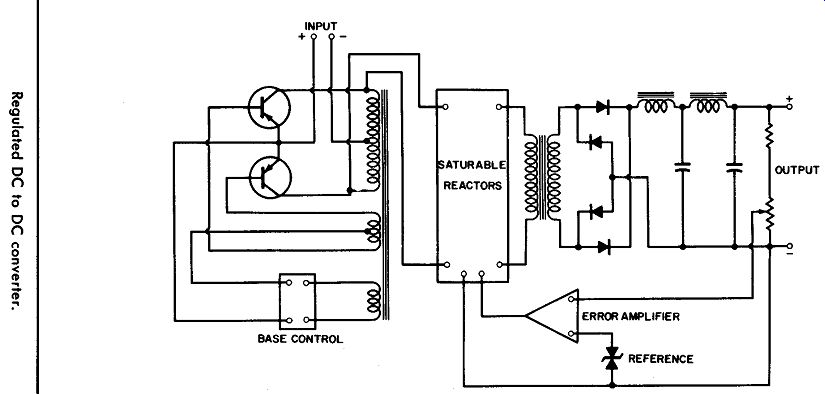
------------ Reg. DC-to-DC converter.
This circuit consists of two PNP power transistors in a push pull switching circuit, which is connected to the DC power source by a control circuit. The two transistors alternately connect the input voltage across each half of the primary of a toroidal trans former. The transistor dissipation is low and the conversion efficiency high. In addition to the primary and secondary, the toroid also has windings for positive feedback from collector to emitter of each transistor.
When one transistor conducts, the supply voltage is placed across half the primary, and the opposite collector is driven negative to twice the supply voltage. At this point the base feedback voltage is reduced. The collector current and voltage across the primary are also reduced, lowering the base drive. This action regeneratively shuts off the conducting transistor and starts the conduction cycle in the opposing transistor. The resultant wave form is a series of square waves across the primary.
The frequency of oscillation is a function of the characteristics of the transformer core, the number of primary turns, and the supply voltage. A base-control circuit is used to prevent excessive transistor dissipation when the oscillator is effectively operating at no-load. The control circuit also provides quick starting and prevents transistor failure if the supply voltage should accident ally be reversed.
The base-control circuit takes advantage of the reversal in polarity between PNP and NPN transistors. This reversal permits the bases of the PNP oscillator transistors to be connected directly to the collector of an NPN control-transistor circuit and then to the positive end of the DC supply. The control transistor has a negative bias voltage obtained from an additional winding on the exciter transformer. The collector current of the control transistors ( hence, the maximum base current of the oscillator pair) is determined by this bias voltage.
The control transistor has a high effective collector resistance, and the oscillator transistors act as though they were operating with a constant-current bias. Thus, if for any reason the output should become shorted, there will be no bias voltage and the base current will drop very low. This protects the converter from accidental shorted loads, because the other DC power sources are not protected.
Base-circuit regulation may be used; a sample of the rectified and filtered output voltage is compared with the accurate, stable reference voltage of a zener diode. The difference voltage is then amplified by one or two transistors and applied to the base of a regulator transistor in series with the base return circuit of the switching transistors. The control-transistor impedance varies in proportion to the error voltage and thereby changes the output of the switching transistors.
A saturable-reactor regulator may be used between the free running transistor oscillator and load. Saturable reactors are switched, opening or closing under control of an error voltage obtained by comparing the rectified and filtered DC output voltage with the voltage of a zener diode.
SHORT-CIRCUITPROOF INVERTER
A circuit with protection against shorts is shown here. Inverter circuits that use bistable devices often require protection. The low conducting impedance and high efficiency of the control devices make them attractive for inverter use, but faults will develop if the load shorts or opens or if the gate drive is lost. This circuit has been developed to protect the inverter.
The rectifiers perform the inverter function from a 24-30-volt DC supply to a HO-volt, 300-V A, 400-cycle load. The firing mechanism for the gates is a free-running multivibrator. The additional components in the center of the diagram perform the protective function.
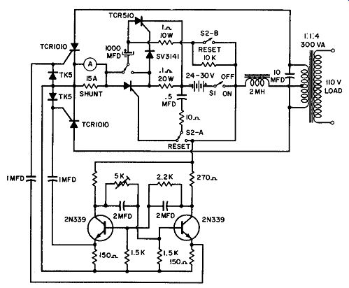
---------------- Short-circuit proof inverter.
To energize the circuit, switch S1 is closed and lever switch S2 is depressed and released. Considering the basic circuit action only, rectifier 1 fires through the DC power source and half of the transformer primary. When rectifier 2 fires, it takes the identical path but uses the lower half of the primary. The flywheel effect of the commutating capacitor, across the secondary, continues this action. When S2 is depressed, switch sections S2A and S2B provide a fast-charging path for the 1,000-mfd capacitor through the 1.0- and 0.1-ohm resistors. Switch section S2C pro- vides a changing path for the 0.5-mfd capacitor through the 10 ohm resistor. When S2 is released, the capacitor provides the charge for the firing of the TCR1020, while the 10K resistor pre vents the charge of the 1,000-mfd capacitor from leaking off.
Assume a short circuit across the load. This would be reflected into the primary, and the commutating capacitor would fail to build up the charge required to maintain the commutating action. The TCR which was conducting ( TC R1, for example) will not be turned off when TCR2 is fired. However, as soon as the drop across the 0.1-ohm resistor exceeds 1.5 volts ( normally 1 volt at 10 amperes average), TCR510 is fired and the 1,000-mfd capacitor places a negative voltage at the anode of TCR1020, turning this device off and interrupting the current flow in the main circuit.
A secondary-current flow momentarily continues through TCR510. However, the l0K resistor in this loop limits the current flow to a value below the holding or minimum sustaining value for current flow. The circuit shuts down completely, but may be reset by depressing SL The same protection is afforded if the gate drive is lost or the load opened.
When solid-state short-circuit protection is not required, the controlled rectifiers may be protected against fault currents by a fuse or fast magnetic circuit breaker. To prevent misfiring when the inverter is switched on, the multivibrator must be switched on before the voltage is applied to the controlled rectifiers, or a slight addition made to the multivibrator circuit to assure its proper starting.
DC-TO-DC MULTIPLIER
This DC voltage multiplier converts 1.5 volts DC to 50 volts DC. By providing a high voltage from a low-voltage source, it eliminates the troublesome vibrator or bulky B+ battery. When the transistors oscillate, they provide an AC voltage across the transformer. The output voltage and current are determined by the battery voltage and transformer turns ratio; therefore, they may be varied to suit the application, as long as the transistor and diode ratings are not exceeded.
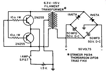
---------- DC to DC multiplier.
OSCILLATOR-AMPLIFIER DC-TO-DC CONVERTER
This oscillator-amplifier circuit can have an input of either 14 or 28 volts. For 14 volts the power output is up to 100 watts; at 28 volts it doubles, to 200 watts.
Transformer T1 is bifilar wound onto an AP 11-424 Ceramag core and yoke with No. 22 Nylclad copper magnet wire. The primary has 108 turns and is center tapped. The secondary also has 108 turns and a center tap, but has two additional taps 13 turns from each side of the center. Transformer T2 can be wound using Arnold Core Section 4 MIL C Core (A)-H-12). BM is equal to 12 kilogauss with an area of 0.5 square inch.
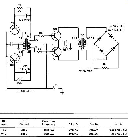
----------- The following parts ore independent of input voltage.
C,C,-0.2 MFD, 200 VOC, c,.C,-500 MFD, 50 VDC, R1R2-100 ohms, 1W, CR1234-1N2614, T2 MTR-916, PX-1301
Oscillator-amplifier DC to DC converter.
When the oscillator is connected, the correct phase relationship between the primary and feedback windings must be maintained.
If oscillation is not obtained and the phase terminals are not marked, reverse the collector or base leads.
From the curves, greatest efficiency ( about 87 % ) can be obtained at 100 watts for an input of 14 volts, and 200 watts for 28 volts.
-----------------------
MULTIVIBRATOR-DRIVEN INVERTER
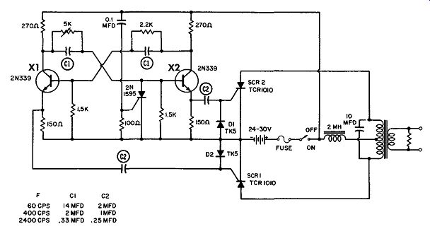
This figure shows a multivibrator using 2N339's and firing a pair of controlled rectifiers. To start the circuit, switch Sl is closed to apply the supply voltage to the CR' s and trigger circuit.
The sudden rise of the supply voltage at the trigger circuit causes a positive spike at the gate of the small controlled rectifier 2Nl595, which fires. The base of the second 2N339 is then shorted to ground and thus prevented from conducting. The first transistor conducts and turns on C R1. When capacitor C1 is charged, the current through the 2Nl595 will drop below the holding current because of the high impedance ( approximately 3K) to the flow of current. This controlled rectifier is thus turned off. When the 2Nl595 is turned off, normal multivibrator performance of the trigger circuit is obtained, resulting in proper starting and normal inverter performance.
The values of C1 and C2 are given for 60, 400, and 2,400 hz.
For better frequency stability, the supply voltage of the trigger circuit may be regulated by using a zener diode.
DC-TO-DC CONVERTER
This converter can be used for a variety of outputs, from 12 to 14 volts DC input at 75% efficiency.
For 250 volts, 65 mils, the transformer is a TY-68S with a pair of 2N669 transistors and 20 square inches of heat sink. Rectifiers are 1N2613's; R1 is 500 ohms, 5 watts; R2, 50 ohms, 5 watts; R3, 300K, 1 watt; C1, 50 mfd, 50 volts; C2 is not used; and C3 is 2 mfd, 400 volts.
Other values-for 300 volts at 100 mils, 325 volts at 200 mils, and 375 volts at 200 mils-are as shown.
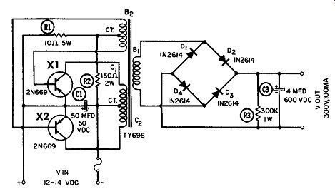
----------- DC to DC converter.
-----------
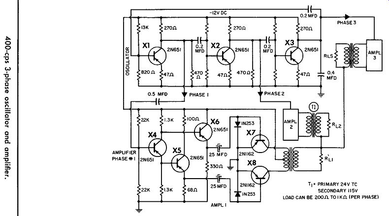
400-hz, 3-PHASE OSCILLATOR AND AMPLIFIER
A circuit for driving a 20-watt, three-phase load at 400 hz is shown here. The three-phase oscillations are supplied by an RC-coupled oscillator so that a 120° phase difference exists at the collector of each transistor. An emitter-follower amplifier drives the output-power transistors into saturation. The result is a clipped sine wave on the output-transformer secondary.
This circuit can be used to drive a three-phase aircraft gyro motor from a 12-volt DC supply.
MULTI-PURPOSE DC-TO-DC CONVERTER
Power converters can be bought as complete "package" units as shown, or special transformers may be purchased separately and a power supply custom-built. A 12-volt transformer can be used in the circuit shown. This unit provides up to 40 watts of output at 200, 250, or 300 volts DC, with current drains of up to 125 ma. Two power transistors are cross-coupled to form an oscillator that operates at about 2 khz. After the voltage has been stepped up, the oscillator is rectified by a voltage doubler and filtered by an RC filter.
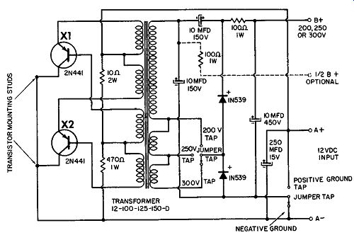
------------- Multipurpose DC to DC converter.
COMPLEMENTARY POWER CONVERTER
As power requirements increase, transistor converters become more complex. More transistors are needed; they may be either series- or bridge-connected. Both circuits usually are transistors of the same type. The transformers for converters are complex, requiring six or seven windings.
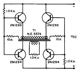
--------------- Complementary power converter.
A complementary transistor converter with a simple circuit is shown. Using complementary transistors results in circuit economy and greater reliability. The transformer uses only two windings. The bases and emitters of the PNP and NPN transistors are in parallel. This prevents the bases from becoming highly back-biased, because if one unit is turned off the other must be turned on. The inherent protection reduces the possibility of self destruction when the transistors are operated with inductive loads. The converter shown has an efficiency of 87% at an output of 122 watts and with a supply of 45 volts DC.