The Mark I-- A Low Distortion IC Preamplifier
/ Control Unit, by Michael Lampton and Donald Zukauckas; Listening
Tests on the Mark I ---by David Vorhis--A well researched, compact, high
performance unit. .
by Michael Lampton and Donald Zukauckas
Michael Lampton and Don Zukauckas
Space Sciences Laboratory
University of California Berkeley, CA 94720
THE ELECTRONICS WORLD is rapidly changing, particularly in the digital and analog design fields. The reason is the tremendous impact that integrated circuits have had on the configuration, performance, and cost of electronic items.
The improvements in IC op amp characteristics in the last two years make it now possible to achieve state-of-the-art performance in an IC audio preamp. In this article we'll discuss a few of the design considerations we must take into account in optimizing preamplifier circuitry, and then describe the details of a preamp design well suited for home construction.
Its performance surpasses most discrete device preamps; the design is simpler and can be cheaper as well. Numerous modifications to add or delete control functions are possible, and we'll point out a few of these as we go along.
What do we expect of a good preamp? Some gain, of course, and a reasonable degree of flexibility in signal switching and control. The preamp is, after all, the control center of the stereo system. We also have every right to expect noise and distortion near the vanishing point. It is in these two areas that some of the simpler designs, including most IC preamps, are deficient. Only recently have op amps become available which combine low noise, high slew rate, and freedom from crossover distortion. These new generation chips make possible the preamp described here.
Another major problem in present-day preamp design is how to reject undesirable subsonic signals which originate most commonly in phono disc warp and can cause serious loudspeaker distortion problems. The provisionally revised RIAA phono playback equalization characteristic permits considerable attenuation in the infrasonic 0-20Hz band.
The Mark One preamp makes full use of this freedom to achieve a large rejection factor for signals in the tone-arm resonance band. This rejection not only helps loudspeakers but considerably eases the dynamic range picture within the preamp and at the power amp down stream.
For several years, many engineers and hobbyists, ourselves included, were apprehensive about using integrated circuit op amps in high quality audio gear.
We lacked firm data and design guidelines relating to op amp distortion and in particular to transient intermodulation distortion. As TAA 's readers are aware, Walt Jung(1l) has accomplished the large task of reviewing the entire field of IC op amp distortion mechanisms and classifying the many available chips with regard to audible and measurable distortion.
Jung's work clearly reveals that the essential ingredient for low distortion performance is adequate slew rate. His rule of thumb is to have sufficient slew rate capability in each stage to allow it to swing from zero to peak in one microsecond: for example, one should allow 10 volts per microsecond for an op amp delivering peak signals of +10 volts.
Actual signals do not have transients this fast, but intermodulation effects start to appear at levels far below the ultimate maximum slew rate of a given state.
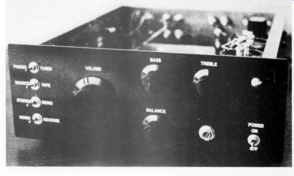
------ Photo A: Front panel of the preamp.
THUMPS SLEW AND NOISE
The IC op amp types which perform well in Jung's distortion measurements and listening tests are those with large slew rates, large gain bandwidth products, and linear output stages. This latter requirement rules out the nonlinear slew rate boosters found in a few chip designs.
Among good performers are the National LM318, the similar Analog Devices ADS518, the new Signetics NE5534, and the Harris 2500 and 2600 series devices.
The first three achieve wide bandwidth with reasonable phase shift by feeding the high frequency part of the input signal forward, past the chip's sluggish lateral base pnp transistor, via a small value capacitor built into the chip. The Harris devices use a somewhat more sophisticated dielectric isolation process to create a wideband vertical pnp structure.
All these devices operate from +15 Volt supplies and can swing a 1k load through at least +10 Volts. They all have differential inputs, making them equally easy to use in series and parallel feedback applications. The balanced inputs also permit the use of circuitry having no output DC, so that blocking capacitors need not charge up on turn-on; this avoids a monster output pulse when the preamp is switched on or off. All these op amps have sufficient open loop gain, 90-100dB, and gain bandwidth product, 10-100MHz, to give excellent feedback performance throughout the audio band.
By the way, these values of gain and gain bandwidth product substantially exceed the values obtainable with the simpler discrete-transistor designs. The benefits appear in the form of more tightly controlled frequency response, better rise and fall times, and input/output impedances which more closely approach their theoretical values. Most important, all these op amps have slew rates in excess of 10 volts per microsecond and exhibit inaudibly small slew distortion in audio applications.
The remaining crucial factor in op-amp selection is noise. To make a long story short, the only chip we've found that offers as low a noise level as the thermal fluctuations in phono cartridges and volume control pots is the Signetics 5534.
Our design uses this device. For those of you who aren't so concerned about noise level, any of the devices listed above should be satisfactory.
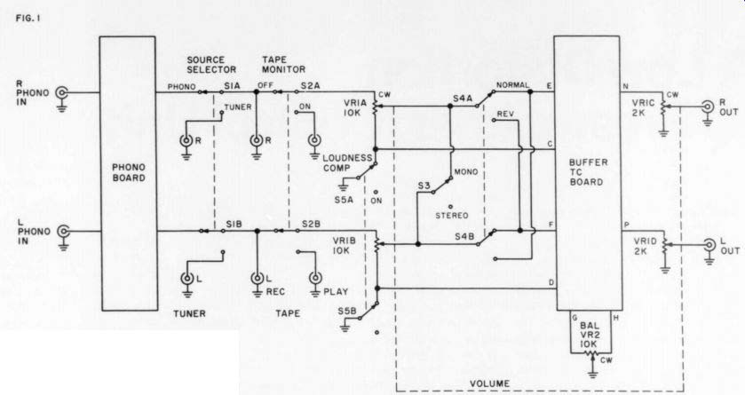
Fig. 1: Block diagram of the Mark One preamp, showing the signal switching
details and the volume control. Tone control detail is shown in Fig.
7. One or more additional switches for external processing loops, wired
like the tape monitor switch, can be added between the tape monitor and
the first volume control gang.
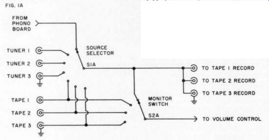
FIG. 1A
Fig. 1a: Alternate signal switching arrangement for handling up to three tuners and three tape recorders. Any tape can be dubbed to any other tape while monitoring either the source signal or the receiving recorder's playback signal. Both the source selector switch and the tape monitor switch must be multiposition shorting rotary types.
This figure shows the right channel only; the left channel is identical and ganged to the right.
------------
TABLES OF COMPONENT VALUES
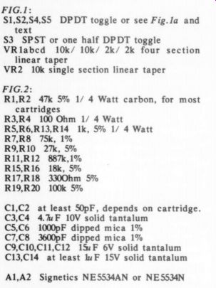
FIG1:
S1,S2,S4,S5 DPDT toggle or see Fig.1a and text
S3 SPST or one half DPDT toggle
VR1_abcd 10k/ 10k/ 2k/ 2k four section linear taper
VR2 10k single section linear taper
FIG.2:
R1,R2 47k 5% 1/4 Watt carbon, for most cartridges
R3,R4 100 Ohm 1/ 4 Watt
RS,R6,R13,R14 1k, 5% 1/4w
R7,R8 75k, 1%
R9,R10 27k, 5%
R11,R12 887k,1%
R15,R16 18k, 5%
R17,R18 3300hm 5%
R19,R20 100k 5% 4 Watt
C1,C2 at least 50pF, depends on cartridge.
C3,C4 4.7uF 10V solid tantalum
C5,C6 1000pF dipped mica 1%
C7,C8 3600pF dipped mica 1%
C9,C10,C11,C12 1%F 6V solid tantalum
C13,C14 at least uF 15V solid tantalum
A1, A2 Signetics NESS534AN or NESS34N
-----------------
ARCHITECTURE
The active circuitry of the Mark One preamp occupies two circuit boards: the phono preamp board and the high level buffer / tone control board. These fit together as shown in Fig. 1, which details the signal switching circuitry and volume control wiring. The phono preamp input connects only to the cartridge, and provides a fixed gain of 40dB with fixed RIAA equalization. Its output is one of several high level inputs to the volume and balance controls and the high level circuitry. The balance control introduces a signal loss of 3dB.
In the high level board, we pick up another 20dB of gain as well as feedback type tone control action. Note that the volume control is a two-stage design, i.e., there are four pot sections on one shaft for stereo. The idea is to provide attenuation both at the input of the buffer amplifier (for best overload management) and at the output (for rock bottom noise at reduced gain settings). This scheme also allows the use of linear taper pot sections, which track better than audio taper sections. The resulting volume control curve is parabolic, which many people feel is superior to the common bilinear approximation found in audio taper pots.
Fig.1 also shows the optional passive loudness compensation circuit: the switchable RC network at the ground ends of the first pot sections. Switched off it has no effect, but oz it provides a modest amount of bass boost at reduced volume control setting. The RC networks are located on the buffer amplifier board.
The signal switching provisions of Fig. 1 are not particularly elaborate. They include source selector, a one-deck tape playback monitor, a stereo normal / re verse selector, a stereo/ monaural switch, and the loudness compensation switch. These control functions can be achieved with five DPDT toggle switches.
To accommodate more signal sources or to adopt a more versatile two or three-deck tape monitor, S1 and S2 should be multiposition rotary or lever switches of the make-before-break (shorting) type.
Some examples of circuit diagrams for these functions are easily found in back issues of TAA(2), and one possible arrangement is sketched in Fig. 1a.
PHONO PREAMP
The phono preamp has a rather specialized job. It must present a controlled load resistance, usually 47k, to the cartridge.
The total capacitance which shunts the pickup also has an important effect on the cartridge's frequency response. Most cartridges are designed for most nearly flat response when loaded by a few hundred pF. We recommend you read Holman's excellent discussion of the cartridge loading problem(3). Suffice it to say that the manufacturer's specified load should be pretty closely followed, and verified with a square wave test record if possible.
In the phono schematic we present the value of the input capacitor C1 should be chosen by subtracting the system cable capacitance from the cartridge's optimum total capacitance. Dynaco preamps have now standardized on 220pF, which we use here as an example.
The preamp's gain should be sufficient to bring a full blast 'zero dB' recorded signal (about 5cm / sec rms referred to kHz) up to a level comparable to the other high level audio signals, say 0.5 volt.
Most common magnetic phono cartridges have gains of about one millivolt per cm / sec, so the preamp gain should be about 100, i.e., 40dB at 1kHz.
A volume control is never employed between the cartridge and its phono amplifier, due to noise considerations. It is thus important that the gain in the preamp be low enough that it will never be driven into clipping, even on the most heavily recorded discs. Studies of phonograph cutting practices(4) have shown that peak velocities of up to 50cm / sec sometimes occur. At least 20dB of headroom should be allowed in fixing the preamp gain. IC op-amps customarily operate from 15 volt supplies and can put out up to 8 volts rms.
So a 40dB gain option looks like a pretty good compromise overall: it offers an 80mV rms input capability, which for a typical cartridge corresponds to the 80cm / sec rms or 110cm / sec peak.
Another design consideration is the occasional presence of large low frequency signals in phonographs, which originate in record warp and in seismic pickup from people walking, dancing, etc. These signals are strongest in the neighborhood of the tonearm / cartridge resonance frequency, typically 7-12Hz. Happ and Karlov have thoroughly researched this problem. These signals must be kept out of the power amp and loudspeaker where they would eat up dynamic range and cause distortion or even damage. The preamp is an obvious place to incorporate a subsonic filter. If we do this at its input or in its feedback path, the filter will not only preserve the power amp and loud speaker but also prevent these low frequency signals from limiting the phono preamp's own dynamic range.
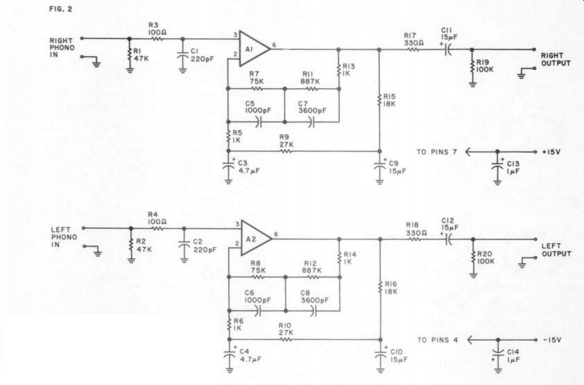
Fig. 2: Schematic diagram of the phono preamp board. Odd numbered components
are in the right channel. Resistors R5 and R6 set the overall gain; 1-k
gives 40dB at 1kHz, RIAA equalized.
Fig. 2 is the circuit we've come up with. The input network, comprising R1, R3, and C1, shunts the cartridge. R1 is the cartridge load resistor; R3 and C1 form an RFI filter at the preamp input. R3 should have a reasonably small value, say 100 ohms, to terminate the input cable and so avoid VHF resonances, and to minimize the total thermal noise in the audio band.
C1 is the cartridge load capacitor, and also provides a low impedance ground path at radio frequencies for the noninverting input of the op amp Al. This feature is important when dealing with op amps which have gain bandwidth products of 10-100MHz: if high frequency impedances are not controlled close to the op amp pins, RF oscillations are a definite possibility. (It is also important to bypass the power supply pins within a few inches of the chip.) So the R3 / C1 network is as important to the op amp as it is to the cartridge.
The feedback circuit around Al controls the gain and frequency response of the stage, employing two negative feedback paths. The principal path, which fixes the voltage gain for conformance with the RIAA characteristic, is via R13, R11, C7, and R7 C5. We calculated this network to give a close approximation to the RIAA curve using commercial RETMA 5 percent tolerance resistor and capacitor values. The exact values desired are: R7 75K, C5 1000pF, R11 884K, and C7 3604pF.
(We suggest the 1 percent values in the parts list as alternatives since recent studies by Stanley Lipshitz show that very small RIAA errors make great differences in listening quality.- Ed.)
We found the values used in the schematic work nicely. The network gives a theoretical closed loop voltage gain of 39.65dB at 1kHz when R5 equals 1000 Ohms. To obtain a lower value of phono gain, increase R5 and R6 and reduce C3 and C4 by the same factor. For instance, 2000 ohms and 2.2 uF will drop the gain by 6dB and double the input overload capability without changing the frequency response.
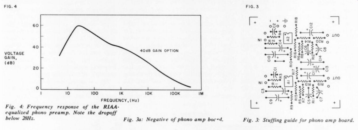
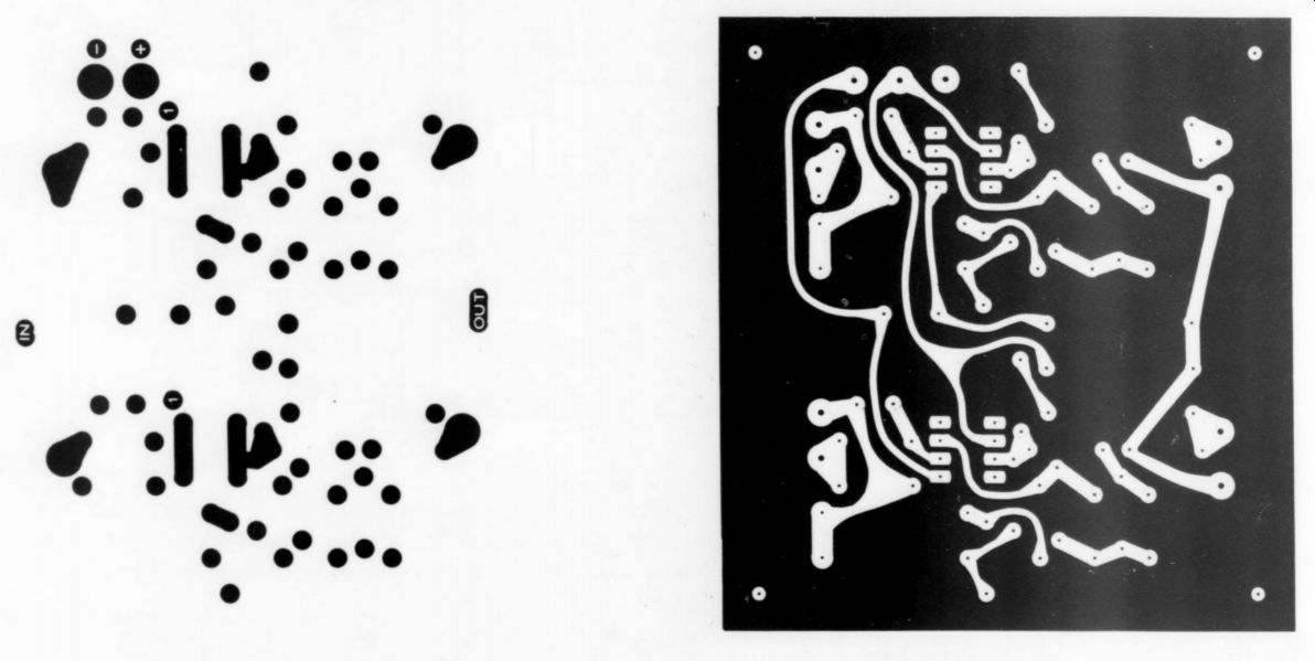
Fig. 4: Frequency response of the RIAA equalized phono preamp. Note
the drop-off below 28Hz.
Fig. 3a: Negative of phono amp board. Fig. 3. Stuffing guide.
Resistor R13 aids the stability of the op amp by keeping the overall feedback factor from approaching unity too closely at high frequencies. Some op amp types are designed to be unity gain stable without external compensation. For those types |, e.g. the LM318 or AD518, R13 is un necessary and could be replaced by a jumper. However, op amps such as the 5534, which are not unity gain stable, demand some attenuation in the feedback loop. The resistor does not affect the closed loop gain in the audio band, but merely provides this desired attenuation at radio frequencies, giving faster settling and less overshoot and ringing on fast pulses. R13's use provides a much better means of assuring good high frequency loop damping than the alternative and more customary method of applying 10-20pF of lag compensation to the op amp, because it does not reduce the slew rate or gain bandwidth product of the amplifier.
The second feedback path comprises components R15 C9 and R9 C3. It controls the subsonic response of the amplifier. The chosen values allow the loop response to conform accurately to the RIAA characteristic down to about 30Hz, beneath which it drops off rapidly enough to give 15-30dB of relative attenuation in the 5-15Hz tone are resonance band.
Specifically, the values shown give a -3dB cutoff at 20Hz and a Q factor of 1. The response has a gentle 0.5dB peak at 30 40HZ, and is 0 dB down with respect to the RIAA curve at 28Hz.
Overall, the shape of this low end cutoff is a compromise between wanting to achieve a flat low end, (i.e., a small Q and a low cutoff frequency) and wanting to achieve a large 10Hz attenuation (i.e., choosing a high cutoff frequency; that, in turn is mitigated by raising Q to about 1).
Our final choice for this network gives almost 18dB of attenuation at 10Hz with respect to the 30Hz point. Our measurements confirm this (see below).
As an option, the 20Hz low frequency cutoff can moved to 10Hz by doubling the values of C3, C4, C9, and C10. This option provides a slightly improved low end amplitude and phase characteristic at the expense of poorer tone arm resonance rejection. This option ought to be satisfactory if a very low-resonance arm is' employed and if the associated loud speakers can tolerate very low-frequency rumble without producing too much distortion.
The fact that we are able to get a satisfactory two-pole high pass filter with a second feedback loop is important: it means we need not employ a cascaded CR or active CR high pass section at either the input or the output of the loop. At the input end, such a circuit is a disadvantage because it degrades the loop's noise performance. At the output end, a high pass filter does nothing to improve the loop's tolerance of low frequency overload although it does, of course, help sub sequent stages. In the present circuit, the low frequency gain is cut by applying increased feedback to the op-amp via the second path, and for the lowest noise this is accomplished at the low impedance (inverting) side of the op-amp's input.
We could achieve some additional low frequency attenuation in the phono circuit by using a smallish output coupling capacitor. That, however, gives a cutoff frequency which depends somewhat on load resistance. We have not used this method, and C11 is large; its job is simply to block the few millivolts of op amp DC offset from reaching the high level switches and pots. The idea is to avoid creating switching transients and potentiometer scratchiness that would occur if the residual op amp DC were not blocked.
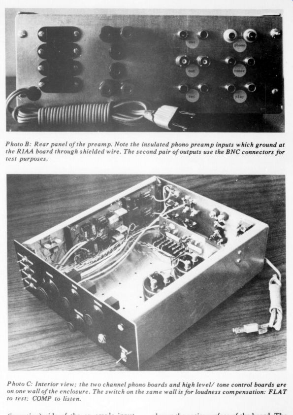
Photo B: Rear panel of the preamp. Note the insulated phono preamp inputs
which ground at the RIAA board through shielded wire. The second pair
of outputs use the BNC connectors for test purposes.
Photo C: Interior view; the two channel phono boards and high level/ tone control boards are on one wall of the enclosure. The switch on the same wall is for loudness compensation: FLAT to test; COMP to listen.
Figs. 3 and 3a show the phono circuit board layout. It uses a double-sided etched circuit board, with one side providing a low inductance ground plane covering almost the entire surface of the board. The other side is etched to produce the usual signal and power conductors. The double sided ground plane idea is borrowed from microwave and fast-pulse technology, where the almost-continuous grounded surface is essential for low inductance signal returns. The layout accommodates all the components shown in Fig. 2 and terminals are correspondingly marked.
We have used 5 percent tolerance carbon composition or metal film resistors, 5 percent dipped mica equalization capacitors, and solid tantalum polar capacitors for the large-value coupling and filtering units. Note that there is no DC drop across any of the signal-path resistors, which means carbons can be used without any excess or “1/ F” noise being generated They will be as quiet as metal film wirewound resistors that is, they will produce only thermal noise. The metal film resistor advantage is tighter tolerance.
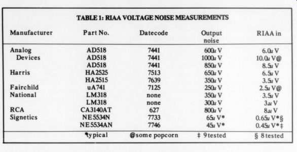
TABLE 1: RIAA VOLTAGE NOISE MEASUREMENTS
MEASURED RESULTS
Fig.4 details our frequency response measurements on the finished board. The RIAA conformance is good overall to within a few tenths of a decibel, depending on how closely the equalization components match their design center values.
Note the 40dB / decade low frequency asymptote, the work of the second feedback path. For these frequency response measurements the signal source impedance was 1-k ohms. With an additional 500mH in series with the signal source to simulate cartridge inductance, the response is unaffected except for the expected high frequency rolloff (which is of course taken into account in cartridge design). This shows the preamp is well behaved when driven from realistic signal sources.
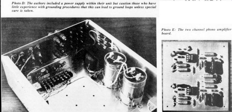
Photo D: The authors included a power supply within their unit but caution
those who have little experience with grounding procedures that this
can lead to ground loops unless special care is taken. -- Photo
E: The two channel phono amplifier board.
One of a low level amplifier's most important characteristics is its noise level. Theoretically, an amplifier's noise performance can be expressed in terms of two kinds of noise sources: a current noise generator shunting its input, and a voltage noise generator in series with its input. In practice, good noise performance will be obtained if these two noise sources are not much larger than the noise accompanying the signal. Achieving this goal in the present circuit is largely a matter of specifying an op amp type with quiet front end transistors.
To compare the various available low distortion op amps, we measured the phono circuit's noise of Fig.2 when each chip type is plugged into the A1 socket.
The results are listed in Table 1. The 'output noise' column gives the false-rms noise at the board's output, filtered to contain only the 27Hz-15kHz band. The 'RIAA in' noise voltages in the table were computed by dividing the output voltages by 100, thus this column gives the equivalent input noise of the amplifier board. For these voltage noise measurements the board's input was grounded. It is clear from the table that, of the units tested, only the 5534 warrants consideration as a low noise chip. The manufacturer's selected low noise version, NE5534AN, is best, but even the unselected NE5534N units tested were extremely good.
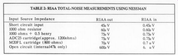
It is also important to measure the degradation of the preamp's noise level when realistic source impedances are connected to the input terminals. The noise level will increase due to the op amp's current noise flowing through the source's impedance, as well as the thermal noise in the source itself. This latter contribution is appreciable: a 1-k ohm resistor at room temperature has an RIAA weighted noise of 0.4 uV. Using one of the 5534's, we obtained the data listed in Table 2 for several different interesting source impedance situations.
In measurements of this kind it is important to use thorough shielding and careful grounding practices, and to visually monitor the circuit's output with a power line synchronized scope to be sure you are measuring random noise and not 60Hz pickup. These data show the 5534 noise level is only 4-5dB above the thermal noise of a typical cartridge. In use, groove noise will entirely mask this. For comparison, 0.52V is 80dB below a 5cm / sec cutting level, or 86dB below an often-quoted 10mV phono preamp input reference level.
TABLE 2: RIAA TOTAL-NOISE MEASUREMENTS USING NE5S534AN
The input impedance is another important operating characteristic. If the op amp were ideal, this would be fixed entirely by the properties of the input network R1, R3, and C1. Measurements with a General Radio 1650A impedance bridge show no difference between the input impedance with the phono amp on and operating and with the chip unplugged from its socket. We measured the loop's output impedance, and it is due entirely to R17 and C11. These measurements confirm the close adherence of the loop's properties to the predictions of the linear network theory on which its design is based.
The phono amp's harmonic distortion is very small. As one would imagine, any op amp offering 94dB of open loop gain at 1kHz (i.e., having a 50MHz gain band width product) will have a huge gain excess in the present phono circuit; due to the shape of the RIAA curve this excess will not fall off much as you to higher r lower frequencies. Indeed, we get over 50dB of excess gain all across the spectrum. Walt Jung informs us the 5534 typically gives 0.03 percent THD at 60dB gain. If extrapolation to 40dB is valid, the phono preamp should have only about 0.003 percent THD. Measurements confirm the THD is below the residual in the General Radio 1932 Wein-null distortion meter. In addition, the circuit is laudably free of crossover distortion: a differential scope plug-in connected across the op amp input terminals shows mostly scope noise plus a small sinusoidal error signal.
We also measured the slew rate capability of the phono preamp circuit, using an EH Labs model 103B pulse generator, which has variable rise and fall times. The pulser fed a passive RIAA preemphasis network whose output went to the phono preamp. The raw pulse was also fed to a 50 ohm terminator at the scope input. The EH pulser can put a 10 volt edge onto a 50 ohm load in 10 nanoseconds; this 1000 volts per microsecond slew rate is enough to overload any op amp.
Slew rate limiting in a phono preamp is easy to observe on a scope. The most obvious manifestation is that the preamp's output waveform ceases to be flat topped.
Instead, as the pulser risetime is reduced, the amplitude of the amp's rising edge starts to shrink, while the top of the wave starts to show a characteristic 76usec exponential rise towards full amplitude.
This rise is due to the fact that, although the highest frequency Fourier components of the square wave are lost by slew rate limiting, the lower frequency components are not. This situation was nicely explained in an interesting paper by Preis(5).
We tested a variety of op amps for slew rate capability in the RIAA circuit. The test conditions were rigorous but revealing: we put a 10 volt 1kHz square wave into the preemphasis network and decreased the rise and fall times until the output waveform just started to deteriorate. Only the CA3140 Bi-Fet was wildly asymmetric. The Harris HA2525 was the fastest, closely followed by the 318 and 518. The HA2515 and NE5534 were somewhat slower, but still well in the running as far as Jung's rule is concerned. All except the 3140 could easily deliver ten volts per microsecond.
For input overload tests we connected a Hewlett-Packard 200CD sine wave oscillator to the preamp input and ran up the level until some sort of misbehavior started to appear at the output, usually in the form of clipping. At the highest frequencies it goes into a slew rate overload condition, which keeps the front end transistors busy all the time while the output becomes noisy and jumpy-looking.
This sort of testing is rather gross: to be visible on scope the distortion is probably well on it's way to 1 percent. We plotted the results in Fig.5 using the 5534 with +15V supplies. At 1kHz, the preamp can handle about 90mV rms and its dynamic range is over 100dB.
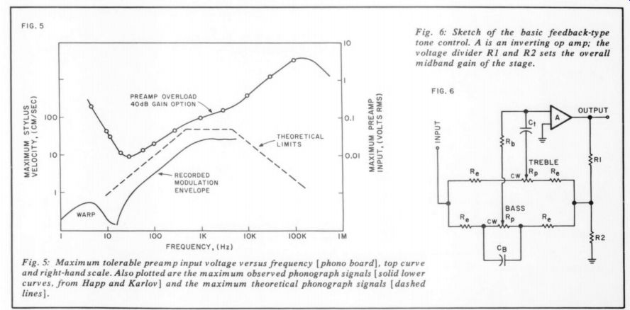
Fig. 5: Maximum tolerable preamp input voltage versus frequency | phono
board), top curve and right-hand scale. Also plotted are the maximum
observed phonograph signals | solid lower curves, from Happ and Karlov]
and the maximum theoretical phonograph signals [dashed lines]. Fig.
6:
Sketch of the basic feedback-type tone control. A is an inverting op
amp; the voltage divider R1 and R2 sets the overall midband gain of the
stage.
Comparing the preamp's input voltage capability with the maximum envelope of phono cartridge signals is informative. We re-plotted Happ and Karlov's data in Fig. 5 assuming a cartridge factor of 1mV / c m/sec. We appear to have plenty of headroom.
We have also sketched in some dotted lines representing three interesting physical limits to groove modulation and stylus motion. On the left is the excursion limit of 0.2mm: this is the peak value of stylus travel which will reduce a one gram tracking force to zero in a cartridge having a compliance of 20X10 cm / dyne.
Thus, above this line your tracking force will disappear at the peaks of the signal. In the middle is a velocity limit of 50cm / sec, typical of the most powerful cutter head output. Above this line the stylus could perhaps track the groove, but present-day grooves do not exhibit more velocity than this. On the right is the acceleration limit of 2x10 6cm/ - sec/sec: this is the value of downward acceleration that one gram of tracking force can, at maximum, give to a 0.5 milligram stylus, i.e., 2000 gravities.
This acceleration limit corresponds to an electrical slew rate of 0.002 volts per microsecond, more than 70dB below the slew rate capability of our preamp. The cartridge will be in serious tracking trouble before the preamp starts to sweat.
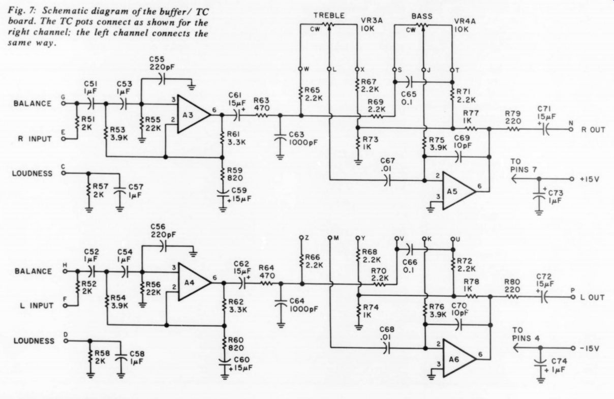
FIG. 7
BUFFER / TONE CONTROL AMPLIFIER
The basic feedback tone control amplifier which has been popular for many years appears to have quite a few advantages over passive networks. In particular, it offers nice symmetrical TC action and requires only linear taper (hence, reasonably accurate) pots. Another feature is that when the controls are centered the gain becomes exactly flat, owing to the symmetry of the network; at least, this is so if the source impedance of the signal equals the driving-point impedance of the loop's feedback network. So with this design a tone defeat switch does not seem essential: flat gain can achieved by setting the knobs to their marked electrical center positions. Another plus is that the loop can be designed to provide some gain, useful in keeping a large dynamic range available at each point in the preamp. In the sketch shown in Fig.6, gain is obtained by attenuating R1 and R2 in the feedback path, with the intent of furnishing enough output swing to insure preamp clipping will never first occur upstream of the TC stage, even when extreme treble and bass cut are cranked in. In the Fig.6 circuit the bass control frequency range is set by the components Re, Rp, and Cb, and the treble control's range by Ct and Rb. The overall midband voltage gain is set by the choice of feedback resistors R1 and R2.
At first sight, it might seem practical to rely on this circuit for the entire 20dB of high level preamp gain. However, achieving low noise with this circuit is not possible if its input impedance is to remain high, because of the unavoidable op amp current noise flowing through the partition impedances Rb and Ct. To minimize the effects of current noise, these impedances must be kept low, which in turn would lead to undesirable loading of signal sources.
TABLES OF COMPONENT VALUES
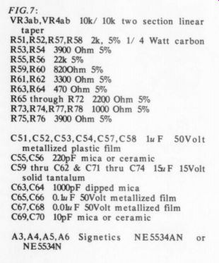
FIG.7:
VR3ab,VR4ab taper
RS1,RS2,RS7,R58 2k, 5% 1 RS3,RS4 3900 Ohm 5% RS5,R56 22k 5% RS9,R60 820 ohm 5% R61,R62 3300 Ohm 5% R63,R64 470 Ohm 5% R6S through R72 2200 Ohm 5% R73,R74,R77,R78 1000 Ohm 5% R75,R76 3900 Ohm 5% 10k/ 10k two section linear 4 Watt carbon CS51,C52,C53,C54,CS57,C58 1uF 50Volt metallized plastic film
CS5,CS6 220pF mica or ceramic CS9 thru C62 & C71 thru C74 1%:F 15Volt solid tantalum C63,C64 1000pF dipped mica C65,C66 0. F S0Volt metallized film C67,C68 0.0: F 50 Volt metallized film C69,C70 10pF mica or ceramic A3,A4,A5,A6 NESS34N Signetics NE5534AN or NE5534N
----------------------
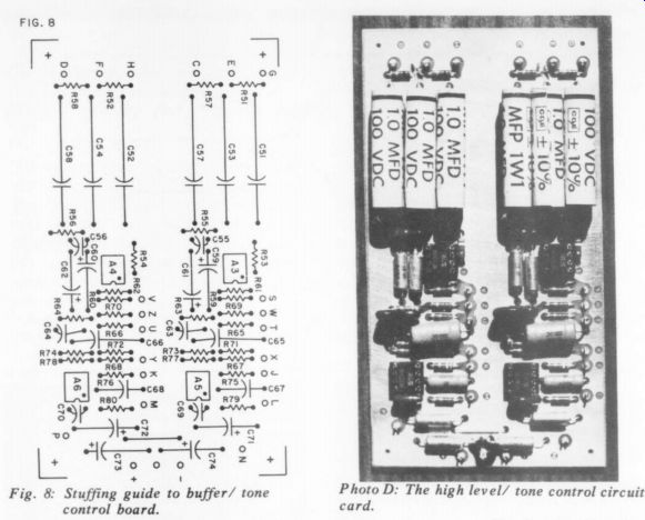
Fig. 8: Stuffing guide to buffer/ tone control board. Fig. 8a: Negative for the buffer/ tone control board.
For these reasons we adopted the two stage design shown in Fig. 7. The first op amp here is a buffer having a gain of 14dB.
Its jobs are to bring the signal level up to minimize second stage noise, and to isolate the signal sources and volume / balance controls from the tone control circuit. In addition to these functions, the buffer includes a fixed three-pole high pass garbage filter(6) which attenuates infrasonic signals in the band below 10Hz. This filter is made up of components C51, C53, C59, and R53, and their counterparts in the other stereo channel. Its purpose is to make life easier for the power amplifier and loudspeaker downstream by removing distortion y 8 causing infrasonic crud which can originate in tape and tuner circuitry and in phono playback. The buffer response is 3dB down at 16Hz. By eliminating this filter, the response can be extended to 3Hz; install jumpers in place of C51, and C60. The response can be extended to DC by replacing C61, C62, C71, and C72 with jumpers. However, we strongly advise against this second option unless the associated power amplifier incorporates a blocking capacitor since loudspeakers tolerate very little DC, and we warn that potentiometers and switches are considerably noisier when op amp DC offsets are impressed across them.
The second feedback loop provides the tone control action and an additional 6dB of gain. Its impedances are kept low for good noise performance and bandwidth.
Indeed, this second loop is flat from DC to 2MHz when the tone controls are centered. Such fierce bandwidth can pose problems for many types of power amplifiers, and our design includes capacitor C69 which rolls off the second loop above 200kHz. Capacitors C55 and C63 serve to control the impedances and phase shifts seen by the op amps, and also restrict the preamp's bandwidth to a few hundred kHz overall. The idea is to ensure loop stability regardless of the source or load impedances imposed on the circuit.
Figs. 8 and 8a give the circuit board layout. The bulky components on this board are the input filter capacitors (1 uF each), for which we have allowed a lead spacing of 1.7'. We recommend metallized plastic film capacitors here, for example the TRW type X463UW 50 volt units. Capacitors of 1000pF and smaller are dipped mica, polars are solid tantalums. Again, carbon composition or metal film resistors can be used.
We measured the frequency response of the buffer / tone control circuit and plotted it in Fig.9. The treble control range is +8dB, while the bass range is +12dB. We chose these ranges for best control feel.
We analyzed the output of the board with the GR distortion meter, and again were unable to detect any THD above the residual of the test equipment. Because these high level op amps operate at closed loop gains of 10-14dB, an extrapolation from Jung's 60dB datum indicates we should expect to find THD figures down in the 0.00015 percent ballpark. Testing with fast-rise square waves indicated a system risetime of about 0.5usec, dependent somewhat on volume and tone control settings. The circuit noise level is extremely low: about 154V rms at the output at full gain, and less as the volume control is reduced. Analysis shows that over half of this noise is nothing more than the amplified thermal noise of the input pots.
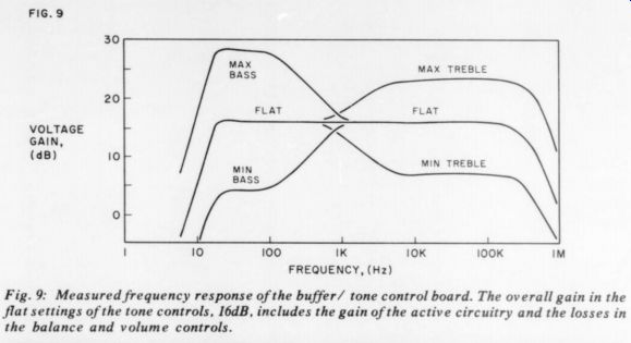
Fig. 9: Measured frequency response of the buffer/ tone control board. The overall gain in the flat settings of the tone controls, 16dB, includes the gain of the active circuitry and the losses in the balance and volume controls.
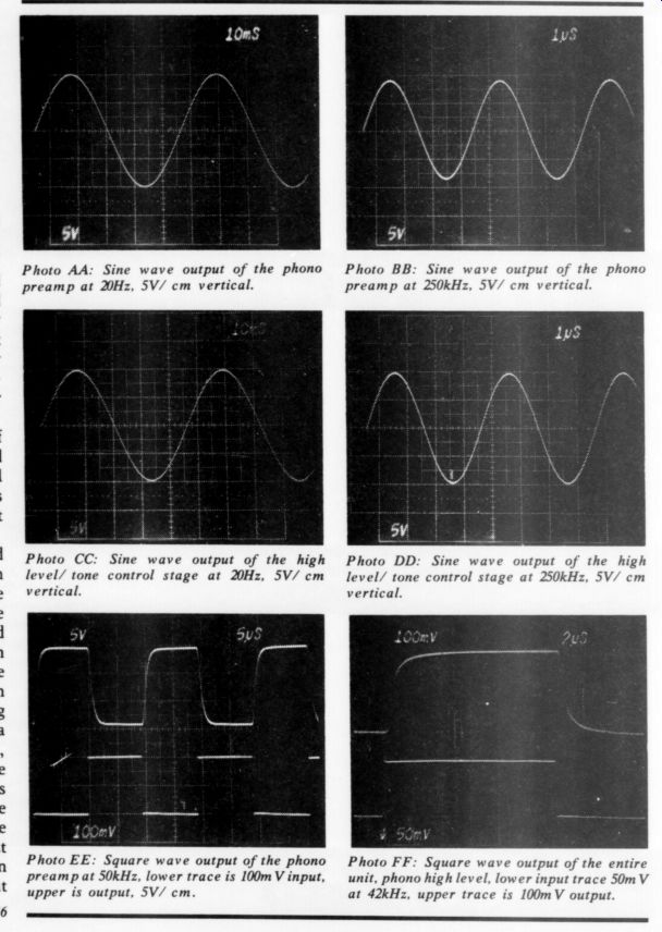
Photo AA: Sine wave output of the phono preamp at 20Hz, 5V/ cm vertical.
Photo BB: Sine wave output of the phono preamp at 250kHz, 5V/ cm vertical.
Photo CC: Sine wave output of the high level/ tone control stage at 20Hz, 5V/ cm vertical.
Photo DD: Sine wave output of the high level/ tone control stage at 250kHz, 5V/ cm vertical.
Photo EE: Square wave output of the phono preamp at 50kHz, lower trace is 100m V input, upper is output, 5V/ cm.
Photo FF: Square wave output of the entire unit, phono high level, lower input trace 50mV at 42kHz, upper trace is 100m V output.
=============
An objective audition of the MARK 1 preamp
I AUDITIONED THE Lampton Zukauckas Mark I preamp very shortly after my examination of the Hafler preamp (see TAA 3 / 78, p. 33). The components used in the tests were basically un changed, and the same reference preamp was used in the comparisons. The latter is a custom tube phono stage which feeds the power amp directly.
By way of background, perhaps I should describe the procedures I used in evaluating both the Hafler and the Mark I.
I first determined the input resistance and capacitance of the phono preamp under test and changed them, as necessary to match my reference preamp. Then I applied power to the preamp for 48 hours before doing any listening.
The listening tests were divided into several parts. I first listened to the phono stage alone, with the output taken from the ''tape out'' and fed to an external volume control and buffer amp. While listening to quality records, I switched back and forth between the preamps at intervals of five to 20 minutes. Volume levels were matched subjectively.
Next, I tested the high-level stage by itself. To do this, I used test instruments to set the tone controls for flat response (in the Hafler they were switched out) and the volume and balance controls for unit gain.
I then wired the test unit, using one of its high-level inputs, into the tape monitor loop of my reference preamp.
The loading of the phono stage in my reference preamp was the same, regardless of whether the test unit was switched in or out. Under these conditions, switching the tape monitor switch on my reference preamp will produce no change in sound quality if the high-level stage is truly perfect. Any change indicates an imperfection.
The other components in the system consisted of a Shure V15 IIIG in a JH Formula 4 arm, a variety of power amps including a Williamson Twin-20, and Fried H speakers. Stax electrostatic headphones and FMI-80 speakers were sometimes used in place of the Fried-H.
The most remarkable characteristics of the Mark I are its smoothness and coherency from the deepest bass to the highest treble. It has no objectionable discontinuities such as the upper midrange ''burr'' in the Hafler. The Mark I simply sounds like the same preamp at all frequencies. The Mark I also never sounds bright or edgy, and is thus free of the most offensive of the solid state colorations.
Of course, no preamp is perfect and the Mark I does have its shortcomings. Its phono stage has a slightly recessed midrange which removes some of the immediacy and presence from the input signal. With several records, these qualities are somewhat restored with an octave equalizer whose 960 Hz and 1.9kHz bands are raised by one dB. In the absence of such equalization, voices appear farther to the rear of the sound stage.
Detailing is quite good at all frequencies, but not outstandingly so. In the midrange, the Mark I's ''musical definition'' is not quite the equal of the Hafler or my reference preamp. In the extreme highs, the Mark I is slightly coarse and not as airy as the above preamps.
The Mark I's mid-bass is not as detailed or as precisely focused as the Hafler.
However, deep bass is more satisfying with the Mark I because it has a more accurate RIAA equalization. Walt Jung and I both commented that Hafler should have included a switch to bypass the sub sonic filter in the phono stage. The Mark I also has a non-switchable sub-sonic filter, but it is a much more successful design: it removes the sub-sonic trash which is present on most recordings without intruding on the music.
The residual noise level of most preamps is high enough to be audible, and bothersome, in my system. The Mark I uses a two-stage volume control which reduces the residual noise in the high-level stage as the control is turned down. In practice, this means that the Mark I high level is completely inaudible at normal gain settings. It is superior in this respect to the Hafler and most other preamps.
However, the subjective sense of dynamic range is no better than most other solid-state amps. The phono stage sounds as if it compresses signal peaks, so that orchestral crescendos are less loud on it than on my tube amp or the Hafler. I do not know what causes this effect; perhaps it is related to the recessed midrange. In any event, most solid-state preamps have this problem (the Hafler is an exception).
The Mark I's high level sound quality is very good. It is neutral and free from any coloration. Switching the high-level section into the circuit results in a slightly softer, more diffuse sound, but it is otherwise inaudible. I should also add that the tone controls and loudness compensation work exceptionally well: they permit subtle adjustment to the extreme bass and treble without affecting the midrange.
In summary, the Mark I makes an interesting contrast with the Hafler. Both are obviously fine preamps, but they do sound different. In fact, their strengths and weaknesses are complementary.
The Hafler is unusually good at reproducing depth and dynamic range. Its principal drawbacks are a bright, somewhat rough upper midrange and poor low frequency response.
The Mark 1 sounds considerably smoother than the Hafler and does not have its equalization or noise problems.
However, the Mark I does not have quite as good depth, dynamics or detailing. The choice between the two depends on one's listening preferences and the associated components. The Mark I is eminently listenable because its imperfections are things it fails to do rather than colorations or distortions added to the input signal. The Hafler, in contrast to the Mark I is more likely to sound offensive if it is used in a bright system.
However, at its best, the Hafler does manage to sound more ''alive.'' Obviously, all of the foregoing comments are directed exclusively to sound quality. A prospective builder should also consider the flexibility of scratch-building the Mark I. For example, you can include as many inputs, outputs and switching functions as you like, or combine the Mark I phono stage with another high level, or vice-versa. In addition, the process of moving from a perceived need to an unique, finished product designed (by you) to fulfill that need provides a satisfaction that no commercial kit can equal.
One last note: the Mark I is based on some of Walt Jung's design principles and ideas and thus should also be compared to Jung's own preamp (The PAT-5 Modification, TAA 1/1978, p. 7). Walt recently agreed to send me one of his prototypes, so I hope to add some further thoughts on the Mark I in a future issue.
Authors' Comment:
We appreciate the careful review Dave bas given the Mark 1, and can only add that the slight phono response irregularity be detected might well disappear in preamps equalized with 1 percent RIAA components instead of the 5 percent in the reviewed unit.
============
The Mark One: A Low Distortion IC Preamp And Control Unit (cont)
POWER SUPPLY
The preamp idles at 5mA per op amp, that is, 30mA at +15 volts DC. The peak consumption is quite a bit higher, roughly 40mA, because of the low impedances involved. A number of existing power supplies can be used to energize the preamp; see for example, the Old Colony lists and TAA's advertiser's ads. For minimum hum, it is best to put the power supply into a separate box and bring the DC into the preamp housing through a three conductor cable as in many other preamps(7).
Another possibility is to steal some DC from the power amp with which the preamp is to be used. In this case, the power amp's main on-off switch becomes the preamp power switch. The low ripple susceptibility of the 5534 allows several millivolts of supply ripple without compromising the preamp's excellent noise performance. Still, filtering is always desirable in the preamp's enclosure to clean up the incoming DC. This filter can be combined with a pair of zener diodes, as shown in Fig. 10, to provide some voltage regulation and overvoltage protection.
The resistors R should have a one or two watt rating and the zener should be rated at one watt or more; or one can employ the newer IC regulators. Be sure the maximum DC voltage available from the rectifiers does not exceed the input voltage rating of the IC regulator.
ASSEMBLY NOTES
Mechanical arrangements for board and connector mounting and front panel design are best left up to the individual builder. Use short lengths of shielded wire to make the internal connections between the boards, control panel, and connector panel. To assure thorough shielding and grounding, the preamp should be enclosed on all six sides by sheet metal, with the PC boards directly grounded to this enclosure by their four corner mounting screws.
The control potentiometers we have used in the Mark One are the Bourns model 81 series modular pots, which are available ganged one to four sections on a single shaft and exhibit good tracking between sections. Get the conductive plastic (not cermet) element option for lowest wiper noise. A good alternate choice is the Allen-Bradley 'mod pot' series 70 family, again available in one through four sections per shaft with conductive plastic elements.
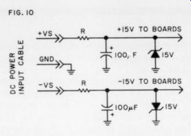
Fig.10: Supply voltages for the preamp can be obtained from an existing
power amplifier having split supplies * Vs if this circuit is mounted
in the preamp housing. The correct value of R is 20x| Vs-15] ohms, for
example, 400 ohms if Vs = 35 volts. The zeners should have a 15 volt
rating at a minimum of 1 watt. The capacitors are not critical.
When first powering up the preamp, monitor the supply currents of the boards to be sure you don't have a wiring error or defective chip. Also check the DC output voltages (pins 6) to verify that there are no bias current problems or open pin 2 or pin 3 connections: all pins 6 should be within a few millivolts of ground.
The only adjustment the circuit needs is the careful calibration of the tone controls for their 'flat' position. The best way to do this is to first permanently mark the front panel with a dot or arrow at the exact 12 o'clock position, directly above the shaft bushing cutouts for the bass and treble controls. Then power up the preamp and apply a 500Hz square wave to a high level input. Be sure the loudness compensation is off or the volume control is at maximum (where the compensation has no effect).
Remove the bass and treble knobs. With a scope, monitor the preamp output and adjust the tone control shafts for best output squareness. Then replace the knobs in their 12 o'clock positions, i.e., aligned with the fiducial marks.
ACKNOWLEDGMENTS
This project is the product of many interested and skilled helpers at UC Berkeley Space Sciences Laboratory and elsewhere.
We want particularly to thank Jan de Vries for his filter synthesis work and Chuck Carlson for his numerous design hints. We finally thank our friend, Walt Jung, for his many suggestions and overall encouragement.
REFERENCES
1. Jung, W., Stephens, M. L. and Todd, C. , TAA # 3, 1977, p. 21.
2. See for example the JC-2 preamp, TAA # 3, p- 48, 1977; also Williams R. D., TAA # 3, 1976, p. 26 and Hayward, T.,TAA # 1, 1975, p. 28.
3. Holman, T., Journal Audio Eng. Soc., 24 # 4, May 1976, p. 263.
4. Happ, L. and Karlov, F., Journal Audio Eng. Soc., 24 # 8, October 1976, p. 630; Holman, T., Audio, 61 # 7, 1977, p.72; Anderson, R., Happ, L. R., Jakobs, B. W., Karlov, F.J., Kogen, J .H., and Mastricola, S.A. Audio, 62 # 5, May 1978, p. 32 and 62 # 6, June 1978, p. 42.
5. Preis, D.,Journal Audio Eng. Soc. Jan/ Feb 1977, p. 2.
6. Jung, W., TAA, # 4, 1976, p. 14.
7. For example, Leach, W.M., Audio, 61 # 2, Feb. 1977, p. 38, or the DB Systems preamp reviewed by Pontis, G., Audio, 61 # 5, May 1977, p. 72.
---------------
AUTHOR, AUTHOR
MANY OF TAA's REGULAR contributors had never written anything for any publication before--surprising themselves mightily by submitting their first manuscript and having it accepted. If you have done a project or have an idea you want to develop and publish, write the editor about it, outlining your idea. He will answer you promptly, tell you whether the idea has already been done, or whether we're interested. We have a handy sheet of suggestions for authors that you are likely to find helpful. Why hesitate any longer?
--------
Also see:
Issues of Reliability and Validity in Subjective Audio Equipment Criticism, by Lawrence L. Greenhill, M.D. Scientific techniques which might improve listening tests
Link | --Link | --The Warbler, by Dick Crawford---A clever test technique for speakers in rooms