by R. Vikan
IN THE SECOND PART of my article I present the audio amplifier stage of this project, along with the steps used to match the FETs needed to construct this stage. I will also detail the circuit board construction and interconnection with the DC-to-DC converter board from Part I, any adjustments and final tests needed to complete this power amp, installing the amp, and making connections for a multiple speaker system.

Audio Amplifier Stage
The configuration of the audio amplifier circuit is a fully complementary design. This circuit is divided into the driver stage and the output stage.
The driver stage itself is divided into two parts, the input and the second stage of voltage gain. The input stage is a symmetrical double differential design using matched FETs. Although using matched FETs makes this stage more difficult to construct, you gain better overall performance. Along with the input stage, the second stage of voltage gain is designed to operate in ...
-----------------
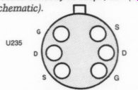
ERRATUM--PART I The pinout configuration for the U235 is incorrectly labeled in Part I (TAA 4/88, p. 18), and the correct version is shown here. Also, capacitor C16 is missing from the DC to-DC Converter Parts List, but is labeled correctly as 100uF, 15V (see schematic).
------------------
... cascode configuration to improve linearity and common-mode rejection. Also within the second stage of voltage gain, a complementary bias-spreading net work provides bias voltage for the out put stage.
The output stage consists of two pairs of parallel MOSFETs that provide the current to drive the speakers.
The input of the driver stage consists of devices Q1-Q5, using Q1-Q3, matched FETs, connected as a double differential amplifier. To reduce the voltage across them, I added dual transistors Q4 and Q5 to the circuit, which converts the differential amplifier to cascode configuration. This improves common-mode rejection, power supply rejection and linearity of the error correcting differential amplifier.
The bias current of the input stage is set at 2mA by constant current source diodes D1 and D2. The gain of the in put stage is set by the source degeneration resistors R3-R6, and collector resistors R7-R10. The voltage drop across R7 and R8 serves as an input for the second stage of voltage gain--a Darlington push-pull cascode circuit.
Q6 and Q7 are the Darlington push pull elements of the circuit, while Q8 and Q9 are the cascode elements. The current through the second stage of voltage gain is set at 10mA by emitter resistors R18 and R19, and the voltage dropped by input collector resistors R7 and R8. The bias-spreading network is between the collectors of Q8 and Q9.
This element within the second stage of voltage gain consists of transistors Q10 and Q11; and resistors R29, R30 and variable resistor VR1, which set up the transistors' operating points. Capacitor C14 provides the AC bypass for the bias-spreading network, which provides a bias voltage of approximately + 3V to the gates of the n-channel output MOSFETs Q13 and Q14, and approximately - 3V to the gates of the p-channel output MOSFETs Q15 and Q16.
These two pairs of parallel MOSFETs make up the output stage. Diodes D7 D10 are connected across the gate and source of the output devices. These diodes prevent an overdrive or short circuit of the output stage from exceeding the gate-to-source voltage of the MOS FETs. Oscillation suppression for this stage is provided by gate resistors, R25-R28.
The idle current in the output stage is set at 100mA (10mV across R33) by VR1. The current through the output stage flows through resistor R33, which is monitored by transistor Q12. As the current through R33 increases, the volt age drop also increases. If the voltage drop increases to the level of 0.6V (6A through 0.12) Q12 will turn on, triggering the peripheral protection circuit (see Part 1). Resistors R31 and R32 set up the operating points for Q12. Resistor R34 monitors the speaker output line for offset volts. Resistor R35 and capacitor C16 form an RC network that provides a load to the output stage at a very high frequency. I didn't use an output inductor in the design of the output stage to provide a better high frequency dampening factor to the speakers.
To null any imbalances, I used a DC servo. The servo circuit consists of IC1, resistors R14, R23 and R24, and capacitors C11-C13. IC1 is configured as a noninverting integrator. R23, R24 and C11, C12 set the cutoff point at approximately 2Hz. R14 determines the upper limits of the DC imbalance the servo can correct. I used an LM308 device for IC1, and added capacitor C13 to improve the rejection of power supply noises.
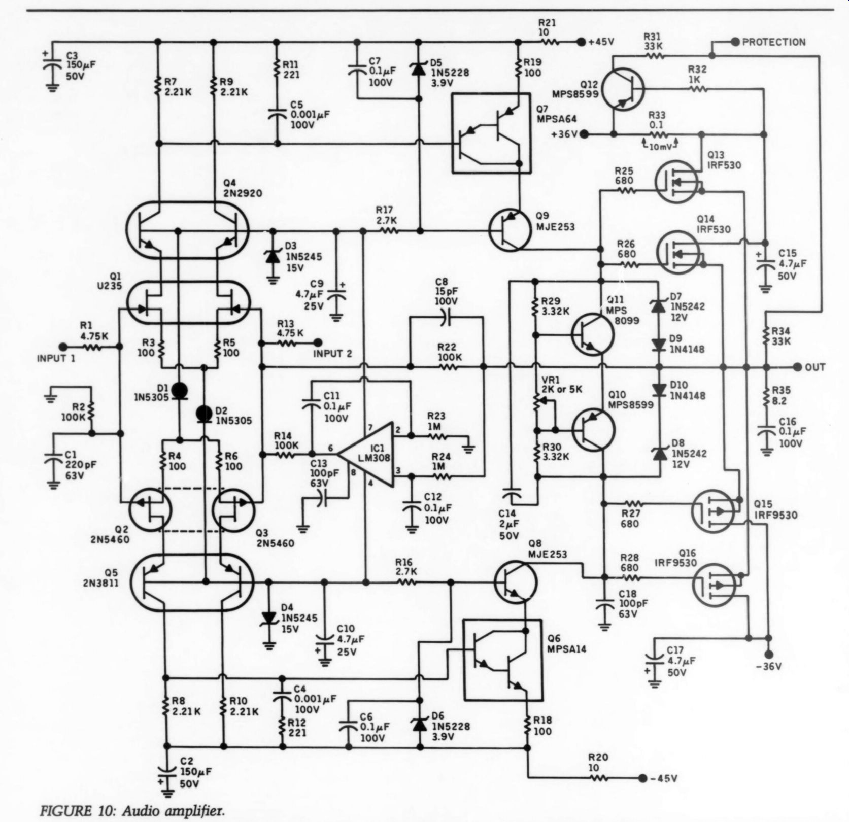
FIGURE 10: Audio amplifier.
The DC servo is powered by the internal biasing string-diodes D3-Dé, and resistors R16, R17 set up the opera ting points for the cascode elements of the input and second stage of voltage gain; and C6, C7, C9 and C10 act to suppress any noise generated in these zener diodes. The biasing string also functions as a power source for the constant current source diodes D1 and D2.
The +45V DC rails from the DC-to DC converter provide power to the driver stage. Any noise from the power supply's +45V DC rails will be filtered by an RC network-R20, R21 and C2, C3. The + 36V DC from the DC-to-DC converter provides power to the output stage. Drain capacitors C15 and C17 bypass the + 36V DC at the MOSFETs of the output stage.
High-frequency compensation is pro vided by two RC networks consisting of R11 and C5, and R12 and C4. These two RC networks reduce the gain of the input stage of the drive circuit at high frequencies. C18 determines the rolloff of the driver circuit. I used C8, an in put compensation capacitor, to ensure the stability of the amplifier. R1 and C1 function as an RC network that keeps unwanted high frequencies from entering the amplifier. R1, along with R2, R13 and R22, control the overall gain of the amplifier, which is set at 26dB.
Matching FETs
Despite what you may believe, matching FETs is not difficult. If you take the time to use the proven step-by-step method I outline, you'll have an amplifier with less distortion and low DC offset.
You may ask, ‘Isn't the DC servo supposed to correct DC offset?' Of course, the DC servo will correct a certain amount of FET imbalance, but be cause FETs have a wide variance in I_pss (saturation drain current measured with Vgs =0) you're likely to encounter Murphy's Law. On the other hand, a little extra time and money will assure optimum performance.
FET Q1 (see schematic, Fig. 10) is already a dual matched FET. However, you must match the two elements in side Q1 with the discrete FETs Q2 and Q3. I suggest you buy a number of Q2 and Q3 (2N5460) FETs and two Q1 (U235) FETs, and proceed as follows:
----------------------
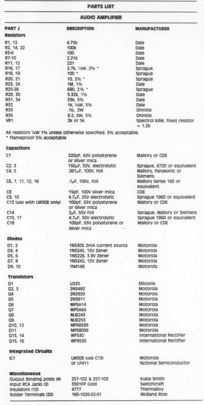
PARTS LIST
AUDIO AMPLIFIER
Resistors R1, 13 R2, 14, 22 R3-6 R7-10 R11, 12 R16, 17 R18, 19 R20, 21 R23, 24 R25-28 R29, 30 R31, 34 R32 R33 R35 VR1
4.75k 100k 100 2.21 221 2.7K, YAW, 2% * 100 * 10, 2% * 1M, 1% 680, 2% * 3.32, 1% 33k, 5% 1K, aW, 5% a9, 2W 8.2, 2W, 5% 2k or 5k
MANUFACTURER
Dale Sprague Ohmite Spectrol 64W, fixed resistor = 1.2k
All resistors %W 1% unless otherwise specified. 5% acceptable.
* Flameproof 5% acceptable
Capacitors C1 C2, 3 C4,5 C6, 7, 11, 12, 16 C8 C9, 10 C13 (use with LM308 only) C14 C15, 17 C18 Miscellaneous
Output Binding posts (4) Input RCA Jacks (2) Insulators (12) Solder Terminals (20)
220pF, 63V polystyrene or silver mica 150uF, 50V, electrolytic 0.001,F, 100V, foil AwF, 100V, foil 15pF, 100V silver mica 4.7uF, 25V electrolytic 100pF, 63V polystyrene or silver mica 2uF, 50V foil 4.7uF, 50V electrolytic 100pF, 63V polystyrene or silver mica -
1N5305 2mA current source 1N5245, 15V Zener 1N5228, 3.9V Zener 1N5242, 12V Zener 1N4148 u23s 2N5460 2N2920 2N3811 MPSA14 MPSA64 MJE243 MJE253 MPS8599 MPS8099 IRF530 IRF9530 LM308 (use C13) or LFa11 257-102 & 257-103 3501FP Gold 4777 160-1026-02-01
Mallory or CDE Sprague, 672D or equivalent Mallory, Panasonic or Siemens Mallory Series 160 or equivalent CDE Sprague 196D or equivalent Mallory or CDE Sprague, Mallory or Siemens Sprague 196D or equivalent Mallory or CDE Motorola Siliconix International Rectifier International Rectifier Motorola National Semiconductor Kukia Smith Switchcraft Thermalloy Midland Ross
------------------------
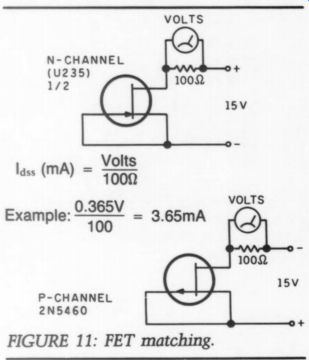
FIGURE 11: FET matching.
Step 1: Measure the Ipss of the two Q1 FETs using the test method shown for the n-channel (Fig. 11). Your measured current will be between 2mA to 4mA. The elements within each Q1 should already match.
Step 2: Measure the Ipss of the Q2 and Q3 FETs using the test method shown for the p-channel; this will range from 1mA to 4mA.
Step 3: For the Q2 and Q3 FETs, choose matched pairs within +0.5mA.
Step 4: Now match the paired Q2/Q3 FETs from the previous step with each Q1 FET. A difference of +0.5mA is an acceptable match between the sets (Q1 and paired Q2/Q3). Don't be overly concerned with achieving an exact match, the DC servo will correct any slight imbalances.
I was able to obtain six matched sets using sixteen 2N5460s and seven U235s; the greatest difference between them was 0.5mA. Using these matched sets, I built three complete amps. With my worst matched set, the DC correction voltage at pin 16 of IC1 is only 2V, well within its range of approximately + 12V.
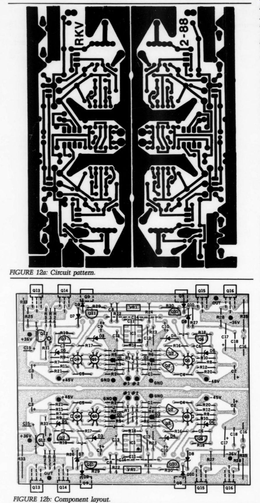
FIGURE 12a. and FIGURE 12b: Component layout.
Amp Construction--- A full-sized circuit board pattern for the audio amplifier stage is shown in Fig. 12a. Refer to the component layout given in Fig. 12b for the installation locations for the components and inter connections.
Begin by installing the twelve jumper wires (J), six per channel, onto the circuit board. Next, install all the resistors, including VR1; be sure R16, R17, R33 and R35 are mounted 1/8-inch from the board since these components run hot. Install C1-C13 and C15-C18, and remember to double-check their polarities where required.
Now, mount IC1, transistors Q4-Q7 and Q10-Q12 and all the diodes. Be sure to check the component layout and the pinout chart (given in Part1) to ensure their polarities are correct. Next, install FETs Q1-Q3; be particularly careful to mount the leads correctly
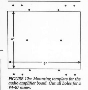
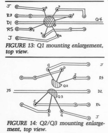
FIGURE 12c: Mounting template for the audio amplifier board. Cut all holes for a
FIGURE 13
FIGURE 14: Q2/Q3 mounting enlargement, top view.
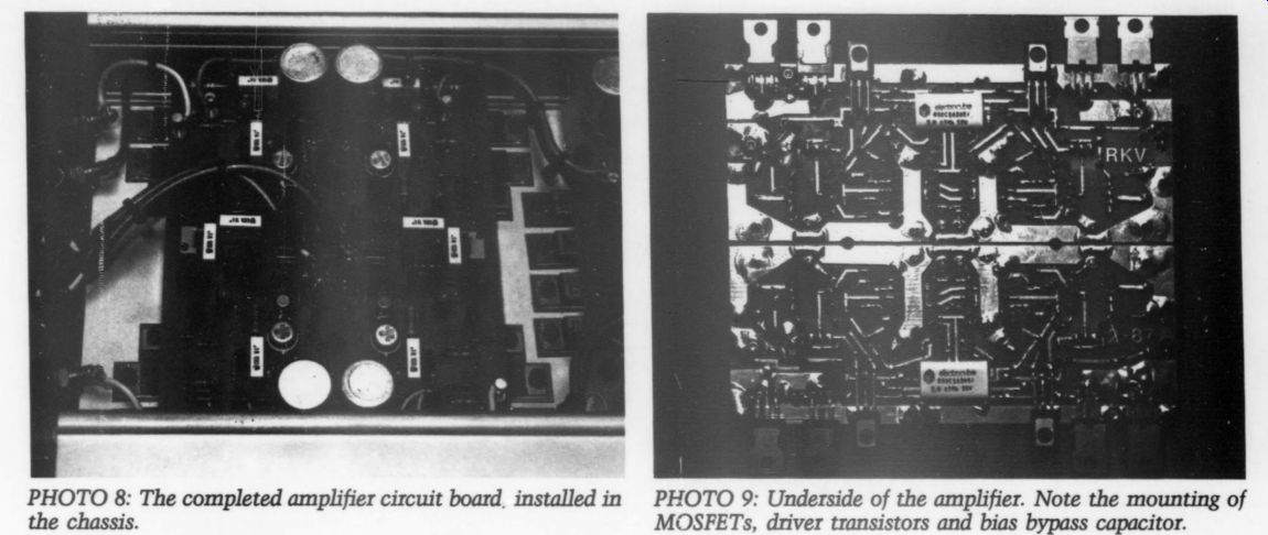
PHOTO 8: The completed amplifier circuit board. installed in the chassis.
PHOTO 9: Underside of the amplifier. Note the mounting of MOSFETs, driver transistors and bias bypass capacitor.
(Figs. 13 and 14). The traces underneath these input FETs are laid out so that a number of different device pinouts can be used.
Finally on the underside of the circuit board, install MOSFETs Q13 Q16, transistors Q8 and Q9 and capacitor C14, mounted approximately 1/16 inch from the underside of the board.
The completed board is shown in Photos 8 and 9.
Internal Interconnections Begin by connecting the + 36V DC and the +45V DC terminals on the DC-to DC converter board to the terminals indicated for each on the audio amplifier board, using 18-gauge stranded wire.
(Refer to Figs. 8b, 12b, and 15.) Next connect the protection terminals on the DC-to-DC converter board to the two protection terminals on the audio amplifier board. Wire gauge here isn't critical.
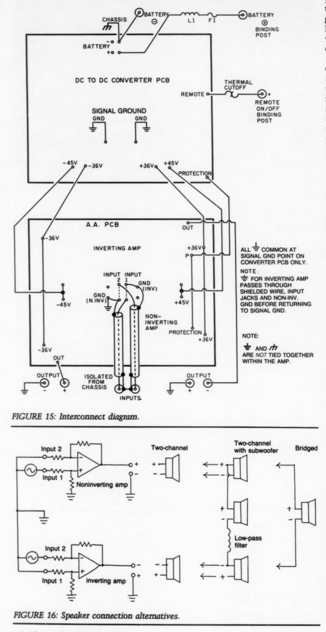
FIGURE 15 ---ALL + COMMON AT SIGNAL GND POINT ON CONVERTER PCB ONLY. NOTE = FOR INVERTING AMP PASSES THROUGH SHIELDED WIRE, INPUT JACKS AND NON-INV. GND BEFORE RETURNING TO SIGNAL GND. NOTE: ARE NOT TIED TOGETHER WITHIN THE AMP.
FIGURE 16: Speaker connection alternatives.
The inputs, outputs and grounds of the audio amplifier can be connected in several configurations, depending on your objective. I designed this board so the terminals of the outputs and grounds can be wired independently.
For example, both channels can be wired inverting, or noninverting, or one channel of each.
I chose the wire my amp with one channel inverting and one noninverting (Fig. 16). With this setup you can bridge the amp to 150W into 8 ohm. To do this, feed each channel with the same input signal and connect the speaker across the two output terminals. The speaker minus goes to the inverting amp out put terminal and the speaker plus goes to the noninverting amp output terminal.
To make the connections for one inverting channel, connect the input 1 terminal to the signal ground (Inv- GND); connect the input 2 terminal to the signal hot (at the input jacks); and connect the output terminal to the negative speaker terminal and the power supply ground terminal to the positive speaker terminal.
To make the connections for one noninverting channel, connect the in put 1 terminal to the signal hot (at the input jacks); connect the input 2 terminal to the signal ground (Inv- GND); and connect the output terminal to the positive speaker terminal and the power supply ground terminal to the negative speaker terminal.
The audio amplifier board was de signed so that there are separate ground terminals for the inverting and noninverting channels. Having separate grounds for each channel allows you the option of choosing the wiring path used to connect the audio amplifier grounds to the power supply grounds.
This allows you to find the best connection for noise suppression.
For my noninverting channel I connected its ground terminal (NInv- GND) directly to one of the power supply ground terminals. I connected the inverting channel's ground terminal by first passing through the shield of its input wire to the common grounds of the RCA input jacks, which are isolated from the chassis, back through the shield of the noninverting channel's in put wire to the noninverting ground terminal, which is already connected to the power supply ground terminal.
Connecting the grounds in this con figuration gives me the best possible noise suppression.
Final Connections
To connect the battery power inputs use a heavy gauge wire and connect the battery negative terminal on the DC to-DC converter circuit board to the battery minus terminal binding post.
Also, connect the battery negative on the DC-to-DC converter board to the heatsink (chassis). Next connect the battery positive terminal on the DC-to DC converter board through the noise filter L1 and the fuse F1 to the battery positive binding post.
Finally connect the remote terminal on the DC-to-DC converter board through the thermal cut-off switch on the heatsink to the remote binding post of the turn-on line. The completed internal wiring is shown in Photo 10.
Adjustments and Tests Mount the audio amplifier circuit board to the heatsink you've selected, using Mica insulators or their equivalent. As you see, I mounted the audio amplifier circuit board next to the DC-to-DC converter board. Figure 12c shows the mounting template. You may choose to mount each board in a separate chassis to increase noise isolation.
Before applying power to the converter, set the bias idle current adjustment control, VR1, to its maximum resistance setting. Temporarily install a 5A (AGC) fuse in the F1 fuseholder.
Connect the battery plus and minus binding posts and the remote line to a car battery or a 30A regulated 13.8V DC power supply. Then, if the fuse doesn't blow, you know you haven't made any major errors in wiring. Check for the +36V DC and the +45V DC at their appropriate terminals (Fig. 15). Also check that the voltage is + 15V at the base of Q4 and - 15V at the base of Q5.
Next, set the idle current by connecting a millivolt meter across R33. Slowly decrease the resistance of VR1 until the voltage reading across R33 is 10mV (100mA idle current). Now check the bias voltage at the collector of Q9, it should be between +3-4V. The negative voltage at the collector of Q8 should be between -3-4V. These bias voltages are not absolute and depend on the MOSFETs you use.
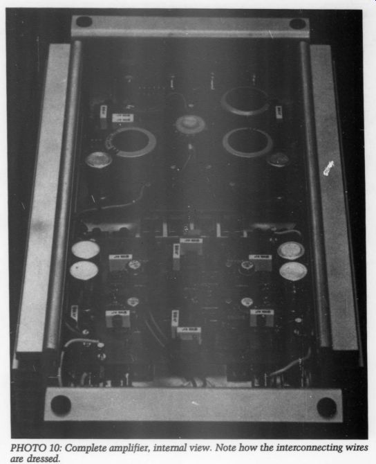
PHOTO 10
Finally, to check whether the DC servo is operating correctly, measure the voltage between each speaker binding post of both channels of the power amp. The speaker output line should read within +10mV of zero. Also check the voltage at pin 6 of IC1. This voltage will be anywhere from +12V DC, depending on the quality of the in put FET match. The closer the voltage is to zero the better.
Without connecting the speakers, connect an oscilloscope to the speaker output and check to make sure you don't have any high frequency oscillations. You shouldn't have any, but if you do, increase the values of R25-R28 to 1k, which should stop any oscillations. Now apply a 1kHz signal to the input jacks and use the scope to see whether it is amplified cleanly.
Finally connect your speakers to the power amp's outputs. Remember to in crease the value of the power input fuse, F1, to 25A before trying any full power tests.
Multi-Speaker Systems The power ground and battery wires should be heavy gauge, such as AWG 8 or 10. This is critical because a lot of current runs through these wires. If you don't use a heavy gauge type you will lose power. The speaker wires should also be heavy gauge, but you can use light gauge wire for the remote line.
Route the power ground and battery wires directly to the car's battery, and connect the remote binding post wire to the power antenna wire of your car's tape deck (Photo 11). Use well-shielded cables to connect the audio input to the preamp output jacks of the tape deck.
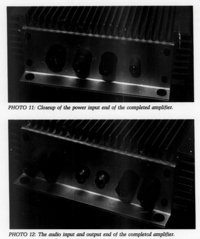
Photo 11; Photo 12
I did not use high level input connections in this design because I believe this type of connection severely de grades the overall performance (Photo 12). Most commercial, high quality, car tape and CD players on the market use low level output jacks, making them compatible with this amplifier.
Depending on the number of speakers you use in your car, you have several alternatives for connecting the speakers to the amp (Fig. 16). Remember, if you have one inverting channel, you must reverse the speaker connections in relation to the noninverting channel to maintain the correct final polarity.
Conclusions
I realize this is a difficult power amp construction project, but I think you'll find it's worth your time. This amplifier will give you quality home amp sound, making all the headaches involved worthwhile. I don't mean to be discouraging, just honest; headaches are involved in any difficult construction project, not just mine.
Like me, perhaps you find yourself listening to your car stereo more than your home stereo. This might be a shame, but it seems that the way life is these days, you spend more ‘free ’ time in your car than at home. Besides, in your car you can crank the volume as loud as you want without irritating any neighbors. It becomes a guilt-free zone. You can turn the subwoofers up until your seat vibrates. Or, to soothe the 'savage beast' when you're stuck in one of those ‘Excedrin headache' traffic jams, you can slip in a mellow jazz or classical tape and ease up on the profanities. So good luck and 'good tunes.’
Addendum
Optional Modifications. In Part I, change the number of the transformer's secondary turns to 11, and tertiary turns to three. Also change C10, C11 to 3,300uF/35V DC (Sprague) and R16 to 36k. See 'Letters' for details.
TABLE 1---SPECIFICATIONS
Power Output:
60W per channel into 8 ohm 75W per channel into 4 ohm 150W (Bridged mono) into 82 Distortion:
Less than .1% at rated output Typically less than .02% at lower output levels (Switcher noise removed)
Frequency Response: 5Hz-50kHz +1dB
Power Consumption: Remote off-15mA Idle-1.8A Rated power-25A
Gain: 26dB
REFERENCES
1. Borbely, E., ‘A 60W MOSFET Power Amplifier, ’ TAA 2/82.
2. Clark B., ‘DC Servo Loop Design For Audio Amplifiers, ’ TAA 3/82.
E. Curl, J., ‘JC-3 Power Amplifier, ’ TAA 2/81.
4. Didden, J.,, ‘Newer Power Amplifier Alternatives: A 200W Version,' TAA 4/83.
5. Jung, W., IC Op-Amp Cookbook, Sams, third edition, 1986.
6. Leach, W.M., 'Build a Double Barreled Amplifier, ’ Audio, May-June 1980.
7. Marsh, R.N., ‘POOGE-3, ’’ TAA 4/85.
VENDORS
Active Electronics PO Box 9100 Westboro, MA 01581 IRFZ30, IRF530, IRF9530, SG2525, MCT271, MCS2400, TLA431, all the transistors required, all diode except IN5305, U235, and 2N5460, Spectrol 64W, resistors 5% and all capacitors except for low-ESR types. $10 minimum charge.
Newark Electronics 500 N. Pulaski Chicago, IL 60624 (312) 784-5100
All MOSFETs required, all transistors, 1N5305, Mallory and Sprague switching supply capacitors, MUR820 and MUR1520, all diodes, binding posts, ICs, most op tocouplers, resistors 1%, JWD-107-5 and magnet wire. $25 minimum charge.
Digi-Key Corp.
PO Box 677 Thief River Falls, MN 56701 All MOSFETs, all types of Panasonic capacitors, 1% resistors and all diodes except 1IN5305.
If readers are interested in this board and/or a kit of parts for it, use Fast Reply #AD130 for the board, or AD134 for kit of parts and board.
-------------------
Also see: