by NORMAN H. CROWHURST
To implement the design theorized in the previous installment, let's draw a schematic and start putting in values (Fig. 1 ) . If we use a collector-to-base resistor for biasing, we make the output-stage current gain depend on output load. Instead, we'll use voltage-divider biasing, so the output stages may be considered as a voltage amplifier, rather than a current amplifier.
The collector load, as discussed in the theory of the previous installment, with nominal external load of 500 ohms and collector resistor of 1K, is 330 ohms. By making the emitter resistor 33 ohms, we set this stage's gain, with nominal load, at 10. Next we decide that the collector voltage should be one third the supply voltage. This will enable a maximum voltage and current swing to be delivered into the external 500-ohm load.
If supply voltage is 12 volts, collector voltage should be 4, with 8 volts, 8 mA in the collector resistor. With our assumed transistor parameters, average current gain 100, minimum 70, maximum 140, the base input current will average 80 microamps, with extremes of 56 and 112 microamps.
With 8 mA flowing through the 33-ohm emitter resistor, emitter voltage will be 0.264 volt. Base-to-ground current should be about 160 microamps, to swamp the 80-microamp average. A resistor of 1.5K will pass 175 microamps at 0.264 volt.
The top resistor must drop 11.74 volts with the average 175 + 80 = 255 micro amps, requiring a value of 47K. Now to check what variation in current gain does. The bias resistors provide an open-circuit voltage of 1.5/48.5 x 12 = 0.37 volts, with a source resistance of 1.5K in parallel with 47K, or 1.45K. When current gain is 70, the base input resistance is 70 x 33 = 2.3K, which will load the base voltage ( which emitter voltage follows) down to (2.3/3.75) 0.37 = 0.226 V. Emitter current is 0.226/33 = 6.85 mA, collector voltage 12 6.85 = 5.15 V. When current gain is 140, the base input resistance is 140 x 33 = 4.6K, which will load the base voltage down to (4.6/6.05) 0.37 = 0.28 V. Emitter current is 0.28/33 = 8.5 mA, collector voltage 12 8.5 = 3,5 V. This is probably an acceptable range of collector voltage variation, from 3.5 V to 5.15 V. The input impedance at the base will average 100 times 33 ohms, or 3.3K. Paralleling this with the biasing resistors, 1.5K and 47K, results in an overall input impedance at this point of almost exactly 1K, with variation due to current gain, from 890 ohms to 1.1K. If this stage uses a 1K collector resistor, its collector load (to a.c. signal) will be 500 ohms, varying from 470 to 525 ohms.
If we use a 10-ohm emitter resistor on this stage, we can set its voltage gain to 50. Now let's put in some signal levels, to figure where we are, and to see what interaction we will get. Suppose the output voltage, with 500-ohm load, is 1 volt rms. Signal input to the output stage base will be 100 mV. Without feedback, the signal voltage to the first stage ( which is the middle stage of our three-stage amplifier) would be 1/50th of this, or 2mV. So the voltage feedback, fed in across 10 ohms, must be 5 times this, or 10 mV, raising the signal at emitter and base of this stage to 12mV. Voltage feedback comes from the 1-volt output point, so the feedback resistor needs to be 990 ohms (1K will be near enough). This won't do, because the 1K in parallel with the existing collector impedance will invalidate our calculations about it. To overcome this, we can use an emitter follower (Fig. 2) . Direct coupling this to the output 1K will present a load of 100K (average) which will not materially disturb the 300 ohms nominal value. It will also transmit the 4-V (average) d.c. voltage, adding 4 mA to the current flowing through the 10-ohm resistor in the middle-stage emitter.
If we reckon on the middle stage taking 6 mA, so its collector voltage is 6 V, the total current in the emitter resistor is 10 mA (average) making the d.c. at this point 0.1 V.
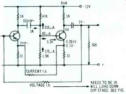
Fig. 1-Development of middle and last stages of amplifier.
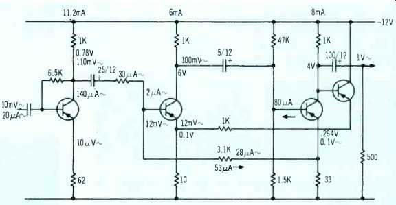
Fig. 2-Addition of emitter follower to avoid undesirable shunting effect
by voltage feedback, and completion of this form of design.
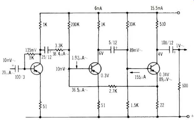
Fig. 3-Eliminating the need for voltage feedback by using different collector
resistor.
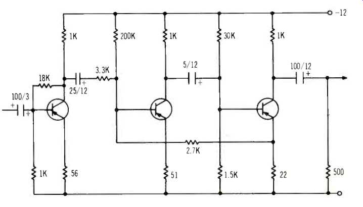
Fig. 4--Change of input circuit to avoid possible blocking by input overloading.
Now we look to the middle-stage base for current feedback. Signal voltage, as already figured, will be 12 mV. Signal current, to produce 100 mV at the collector, with 200 microamps signal current, will average 2 microamps. Voltage feedback should be 14 times this, or 28 microamps, with a signal voltage difference of 100-12 = 88 mV. This combination requires a resistor of 3.1K. Now to figure the d.c. working condition of the middle stage. The output stage emitter voltage is 0.264 V (average). The middle-stage emitter voltage is 0.1 V. So the current feedback resistor will have 0.164 V across it, passing 53 microamps. The average bias current required by this stage is 60 microamps, so this should be adequate to maintain this transistor in its operating range.
At this point, signal, with nominal output load, is 12 mV at 30 microamps, representing an impedance of 400 ohms.
When output is short-circuited, voltage feedback disappears, so signal is 2 mV at 30 microamps, representing an impedance of 67 ohms. When output is open circuited, feedback voltage will be 3 times as great, or 36 mV, representing 1.2K. To swamp this variation in input impedance of the middle stage so it receives substantially constant current from the first stage, a coupling resistor of 3.3K, rather than the 1K suggested in the previous installment, should be used. We have gain enough to spare. Now we redesign the first stage.
With a signal current of 30 microamps at 110 mV ( the input end of the 3.3K resistor) and using a 1K resistor for the first-stage collector, signal current at this point will be 140 microamps. Now we decide the input should be 500 ohms, with input voltage 10 mV, current 20 microamps, which will represent 40 dB insertion gain.
To get 140 microamps collector signal current, the base input signal current needs to be 1.4 microamps (average rms). So the feedback resistor must take the other 18.6 microamps, incidentally increasing collector signal current to 158.7 microamps. This resistor passes 18.6 microamps with a signal voltage of 10 + 110 = 120 mV (phase reversal in stage), requiring a value of 6.5K. Assuming current gain is 100, the d.c. resistance of the transistor at operating point will be 1/100th of 6.5K-about 65 ohms. In series with a 1K collector resistor, this sets the collector-to-emitter voltage at 0.085 x 12 = 0.78 V, which is plenty for handling a 10 mV signal. Now for the emitter resistor.
The drop must be 10 mV signal with signal current 158.7 microamps, requiring 63 ohms. A 62-ohm resistor will probably serve. That was a good exercise in figuring out a fairly complicated feedback situation. But if we look closer, there is a simpler way: why not use a 500-ohm collector resistor on the output stage, so no voltage feedback is needed, then apply 26 dB of current feedback? We use (Fig. 3) a 510-ohm collector resistor, again with 4 V at the collector (based on average current gain of 100) . Using a 22-ohm emitter resistor, with 250 ohms collector load, the stage voltage gain is 11.3. Collector current is 15.5 mA, emitter voltage 0.34 V. Base current will average 155 micro amps. A base-to-ground resistor of 1.5K, with 0.34 V will average an additional 227 microamps, totaling 383 microamps, with 11.66 V, requiring 30K for the top resistor. Base input resistance is 2.2K paralleled by 1.5K and 30K, resultant 865 ohms. Now a 1K collector resistor makes a collector load of 463 ohms.
If we use a 51-ohm emitter resistor, the voltage gain is about 9, so the two-stage gain (middle and output )is close to 100. Now for current feedback.
The output emitter will have a signal voltage (for 1 V output) of 1/11.3 = 89 mV. Previous stage emitter and base will have, in opposite phase, 10 mV. Total 99 mV-near enough 100 mV. Middle-stage collector signal current, into 463 ohms, at 89 mV, must be 192 micro amps. So required base input signal current must average 1.92 microamps. To get 26 dB feedback, the feedback resistor must take 19 times this, or 36.5 micro amps.
A current of 36.5 microamps, and a voltage of 100 mV, requires a resistor of 2.7K. This will stabilize the gain of these stages and linearize gain tremendously.
Now for this stage bias. Output emitter 0.34 V, previous stage, with 6 mA, 0.3 V d.c. We may consider these voltages as the same, essentially, in which case no d.c. flows either way. Actually a small d.c. will flow, to compensate for d.c. gain deviations.
The base bias current requires to be 60 microamps, with which assumption, variation between 70 and 140 for middle stage gain will keep collector voltage well within operating range, and bias resistor drops 11.7 V, requiring a value of 200K. Signal input to the middle stage is now 38.4 microamps at 10 mV, representing an impedance of 260 ohms. Again using a 3.3K `padder', this drops a signal voltage of 125 mV, making 135 mV signal at this collector. A 1K collector resistor will take 135 microamps signal current, making a total at this point of 174 microamps from the first stage.
Again setting the 10-mV, 20-microamp signal input requirement, base input current needs to be 1.74 microamps, feedback current 18.26 microamps, voltage across the resistor 135 + 10 = 145 mV. Value 8K. Emitter resistor signal current 192 microamps, voltage 10 mV, value 52 (use 51) ohms.
This circuit allows plenty of margin for the predicted gain variations. Finally we need to put in capacitor values. Assuming the 3-dB low-frequency point should be 2 Hz, the output coupling capacitor should have a reactance no greater than 1K at 2 Hz, which would require 80 µF. A 100-µF, 12-V capacitor will serve in both circuits.
For the interstage in the circuit of Fig. 2, the capacitor feeds between 1K resistors again, so it needs to have a reactance of 2K maximum at 20 Hz. We want full distortion reduction down to 20 Hz, and the 26-dB feedback will extend the turnover point down from 20 Hz to 1 Hz. This requires a 5µF capacitor.
Now for the capacitor between input and middle stage. In each circuit, this feeds from 1K into about 4K total, so requires a reactance of 5K at 2 Hz. For this, 20 µF would be adequate, but a 25 µF will give some margin.
The input capacitor, like the output, works between two 500-ohm impedances, so 100 uF should be used. As the base is above ground, negative should go to base on the input capacitors, for the other capacitors, negative should go to collector.
In both these circuits, only one capacitor is contained within the feedback loop, so there is no stability problem.
Also no base, except the input stage, has a very high impedance so that a peak can push it beyond cut-off and cause blocking that has a long time delay before operation is restored. If there is any risk of a peak seriously in excess of the rated 10 mV input level, it may be well redesign the input stage with a base-to-ground resistor.
With a base-to-ground resistor of 1K, the base input impedance must be adjusted to 1K, so the combination makes 500 ohms (Fig. 4). The 1K resistor will take 10 microamps of the input signal current, so the transistor must deliver its required output from 10 microamps input, instead of 20 microamps in the previous figuring.
So the feedback current needs to be 8.26 microamps, instead of 18.26, setting the value at 18K. The emitter resistor passes a signal of 182 microamps at 10 mV, for which a 56-ohm resistor is satisfactory. This change has another advantage: it will work the input stage at lower current, giving a larger margin of voltage swing in the other direction.
In the last two articles of this series, we have taken what could have been a rather complicated design, and finished up with a fairly simple and highly stable circuit. The problems were resolved fairly simply--at least it seems so afterwards, but then most problems do! In later articles, we'll explore some other avenues of transistor-circuit design.
(adapted from Audio magazine, May. 1970)
Also see:
Negative Feedback by Norman H. Crowhurst (Apr. 1970)
More on Negative Feedback (Feb. 1970)
Transistor Oscillators (Jun. 1970)
The Function Generator (Nov. 1970)
= = = =