As general service instruments, there are two basic forms of vacuum tube testers. The least-expensive unit tests for emission of electrons from the cathode of the vacuum tube, and is called an emission tester. The other applies prescribed voltages to each element of the tubes and is able to measure the G_m -- it is called a transconductance tester. And among transconductance testers there are two types, one performing a static test and the other a dynamic test, the second including an AC signal source for the amplification test.
All tube testers also perform other tests on tubes, such as testing for shorts between elements, tests for leakage between heater and cathode, and most also include a test for grid current. Grid current will sometimes result from the contamination of the grid by the bombardment of electrons on it from the cathode, or from a tube becoming gassy.
Tube testers have a number of sockets, each to take a different tube pin arrangement. The common elements of each socket terminal are wired together. A multi-tap filament transformer connects to a multiple tap switch for selecting the right heater voltage. A bank of switches (one switch for each tube element) sets up the element connections for each tube. A common plate supply becomes self-rectifying through the tube under test. A milliammeter is in series with the plate supply, the cathode, and the other elements of the tube. A variable resistor across the meter is controlled from the front panel. The meter reads "Good-?-Bad" and, in the case of transconductance testers, includes Gm in micromhos. A chart is supplied by the manufacturers with information on setting the element switches, filament voltage, and "plate load" (so-called, but really only a current-adjusting resistor across the meter in the case of emission testers). The chart settings are made by the manufacturer from "bogey," or selected ideal tubes the instrument manufacturer gets from the tube manufacturer.
In an emission checker all the elements from the grid to the plate, inclusive, are tied together. When the variable resistor across the plate milliammeter is set to the number indicated by the chart, pressing the TEST button applies voltage, and the meter will indicate whether the current capabilities or electron flow from the cathode is as much as it should be, is questionable, or is too low for that tube. Assuming no loss of vacuum or contamination of the grid, the result of aging on a tube is loss of electron emission from the cathode. An emission test, therefore, is an indication of age, one of the biggest reasons for tube replacement.
TRANSCONDUCTANCE TUBE CHECKERS
Transconductance or mutual-conductance testers are more complicated and more expensive. They connect the elements of the tube and apply voltages as they would normally be applied to an amplifier, and include a bias voltage on the grid. When the levers and dials are properly set and the TEST button is pressed, the plate meter reads the tubes mutual conductance (Gm) which is a measure of tube gain.
Mutual conductance (also called transconductance and plate trans conductance) is a combination of the amplification factor and the dynamic plate resistance of a tube. The formula is:
G_m = μ / r_p
Amplification factor (the symbol is μ) is the ratio of a change in plate voltage to a change in grid voltage. Dynamic plate resistance equals the plate-voltage change divided by the resultant plate-current change:
r_p = delta Eb / delta Zb
where,
r_p equals dynamic plate resistance,
delta E_b equals change in plate voltage,
delta I_b equals change in plate current.
G_m may also be defined as a small change in plate current divided by a small change in grid voltage with plate voltage held constant. This more correctly defines dynamic mutual conductance. This is measured only by the best of tube checkers; most mutual-conductance testers check with fixed voltages and perform what is called a static test.
The figure for mutual conductance is in mhos (the inverse of ohms, and is ohms spelled backward). Actual figures for mho is in small fractions, so the scale is marked in micromhos, or millionths of a mho.
A better test of a vacuum tube, therefore, is on a mutual-conduct ance tube checker, with the dynamic mutual-conductance test preferred. Even this is not a positive assurance the tube will work in a particular circuit. It is still possible that the tube will not work as an oscillator, or as an amplifier at very high frequencies. The final evaluation is how it performs in the circuit for which it is intended. A check on the tubes in a tube checker does reduce the possibility of circuit malfunction being due to the tube or tubes.
IN-CIRCUIT TUBE TESTING
Tubes are easily checked while in-circuit by knowing the operating characteristics. Tube manuals give the information. Section 1 described voltage checks that can be made at the grid and plate of a tube. By these checks a tube can be evaluated for current, which proves emission as well as other operating parameters.
SEMICONDUCTOR TESTING
There are a number of instruments for testing diodes, transistors, and other semiconductors. The less-expensive instruments test for leak age, and relative transistor alpha and beta. The more expensive ones include a test for high-frequency cutoff.
Semiconductors do not emit electrons from a cathode or any element, so the most important function of a vacuum-tube tester does not apply to testing semiconductors. Transistors have indefinite life if not abused. Operating them beyond their rated limits will usually destroy them. From a practical standpoint, therefore, the average ham wants to know if a diode or transistor is good or bad. Simple checks take simple instruments.
CHECKING DIODES AND TRANSISTORS OUT OF CIRCUIT
An ohmmeter is a handy instrument for checking out a semiconductor as to whether it is good or bad. It will also check leakage. It will not give you gain measurements, but only tell you if the device is open or shorted.
Semiconductor devices have rectifier action. That is the secret of diodes particularly. Current will pass in one direction more easily than the other. Therefore, comparing the current in one direction with the current in the other indicates, to a degree, the quality of a diode or transistor.
The first thing you must do is determine the voltage polarity of the leads out of your VOM or VTVM in the ohmmeter function. As explained in Section 1, the ohmmeter function is a battery in series with resistors. In VOM's the ground lead is positive ( + ) and the red lead negative ( - ). In VTVM's it may be reversed. Check the schematic of your instrument to ascertain which polarity of the battery goes to ground.
Start with a diode. With the positive lead connected to the anode and the negative to the cathode, your VOM or VTVM should read a low value. The amount of resistance measured will vary with the diode and with the range selected on the ohmmeter. Now reverse the connections to the diode. You should read infinity or nearly so on silicon diodes, and several hundred thousand ohms on germanium diodes. This is a measurement of reverse leakage, and it will be higher for silicon diodes. A low reading means high leakage, and the diode should be rejected.
The forward reading ( + to anode, - to cathode) will vary depending on the range being used. At the beginning of conduction, diodes are not linear. A typical curve looks something like Fig. 3-1. There is ...
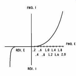
Fig. 3-1. Typical characteristic curve for a semiconductor diode. Note nonlinearity
of curve at low current values.
... very little forward conduction below the knee of the curve. (There is even less in the reverse direction until you get to the point of avalanche where current increases quite suddenly. This is the phenomenon used for zener diodes.) You can calculate the current drawn in the forward direction by remembering the theory of the ohmmeter.
The internal resistor in series with the battery is the center-scale reading times the range-multiplier figure. If the center scale is 10 and you are on the X 1 range, the internal resistor is 10 ohms. If you are on the X 100K ohms range, the internal resistor is 1 megohm (10 X 100,000 = 1,000.000)
Let's take an example. A good "top-hat" power-type silicon diode, the IN 1653, will measure infinity in the reverse direction. It measures 200,000 ohms on the X 100K range and only 9.5 ohms on the x1 range, in the forward direction. How much current is it passing? On the 100K range, the total resistance is 200K (the amount measured) plus 1,000,000 (the internal resistor), or 1,200,000 ohms. Dividing 1.5 (the battery voltage) by this value is 1.25 microamperes. On the x1 range the total resistance is the 9.5 ohms measured plus 10 ohms for the internal resistance, or 19.5 ohms. Dividing into 1.5 volts, the current is 77 mA. At 1.25 uA there is hardly any conduction and the internal forward resistance is high. At 77 mA the current is in the range of normal operation for this diode. This condition is true for all diodes although the ratio between high and low current may not be as great, and will not be as great for germanium diodes, especially the small-signal types. On small-signal diodes it is possible to exceed the current ratings when on the x1 range and destroy the diode. You are pretty safe in using the x10 range, and all that is important is that there be a reasonably high difference between forward and reverse measurements.
TRANSISTORS
The same method is used to check whether a transistor is passable or bad. You can tell if it should work or not work, but not how well it will work. In transistors you have 6 combinations of connections--3 combinations each in two directions of current. On silicon transistors the resistance between collector and emitter will be high (ohmmeter reading nearly infinity) in either direction. On germanium transistors the readings will be fairly high, but higher in one direction than the other. The more important test is between base and collector and base and emitter. In the forward-current direction the resistance readings should be fairly low as compared to the reverse-current readings.
Again the actual reading will depend on the ohmmeter range being used. A zero reading means the element is shorted, and an infinite reading that the element is open. The actual gain of the transistor can not be determined by an ohmmeter test. Again, it is necessary to use caution against applying too much current to the base in the for ward direction. In operation, the base bias current is in the range of microamperes (uA); they are just not built to take too much current.
Keep in mind that whether you are applying forward or reverse current depends on whether the transistor is an NPN or a PNP type.
An easy way to remember forward-biasing polarity is that the center letter is the required battery polarity for forward biasing when applied to the base. An NPN transistor requires a positive ( + ) voltage applied to the base and a PNP transistor a negative ( - ) polarity to the base. In schematic diagrams the emitter arrow points to the outer circle on an NPN transistor, and to the base vertical line on a PNP transistor. The arrow points in the direction of current flow but opposite the direction of electron flow. This adds a bit to the confusion ...
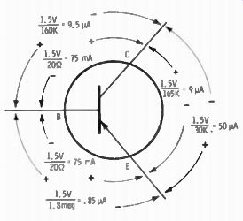
Fig. 3-2. The results of testing an unmarked transistor with a VTVM having
an ohmmeter battery of 1.5 volts.
... about in what direction electricity flows. The arrow points in the direction of the movement of "holes" in semiconductors, and hole drift is called current in this case.
Fig. 3-2 shows VTVM readings on an unmarked transistor. Note the very low resistance (and dangerously high current) when forward biasing voltage is applied between either base and emitter or base and collector.
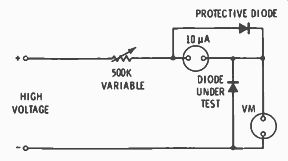
Fig. 3-3. The hookup for a P1V test on a silicon power rectifier diode.
DIODE MEASUREMENTS
Small-signal diodes used as detectors need only to show good for ward-to-reverse current ratios. The check for this is with an ohmmeter as described previously.
Power-supply rectifiers are another thing. The important parameters are the current-carrying capacity, and the peak-inverse-volt age limit. The maximum current rating is the current the diode can carry without overheating the junction internally, with consequent destruction of the diode. The peak inverse voltage (called PIV for short) is the highest reverse voltage that can be applied without break down. Approximate measurement of these parameters can be made by the amateur with a minimum of equipment.
For a PIV measurement you will need a source of high voltage (the amount depending on the rating of the diode), a microammeter, a variable resistor for adjusting current, and another diode for protecting the meter against excessive current flow. The circuit is shown in Fig. 3-3. Say you have a number of "top-hat" silicon rectifiers. Most of them have a PIV rating of 400 volts, and a forward-current rating of 750 mA. Your power supply should be able to produce about 500 volts output. Connect as shown in the sketch. The diode under test must be connected in reverse polarity. Start with the full resistance of the variable resistor. The microammeter may read around 10 uA, with only a slight rise as you reduce the value of the series resistor. Watch the meter carefully. As soon as the meter begins to show a rapid rise in current, note the voltage across the diode and immediately shut off the power. The voltage across the diode before a fast current rise is the PIV rating.
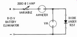
Fig. 3-4. Hookup for checking power rating of diodes. Voltage across the diode
times current through it is the power dissipation. If the figure is higher
than the published rating, discard the diode.
The forward-current test requires a low-voltage, high-current supply. (Fig. 3-4). A battery eliminator is a good one. The series resistor must have a high current rating. A 200-ohm. 200-watt variable resistor is required for this diode example. As you turn down the resistance value, watch both the ammeter and voltmeter, until the product of the two equals the wattage rating of the diode. The rectifier mentioned for this example may have a 1-watt rating. On this basis, the voltage across the diode would be about 1.5 for a current of 750 mA. If the voltmeter reads higher than 1.5, discard the diode.
Higher-rated diodes will have a lower internal resistance, and voltage across the diode will be something less than 1.5. The higher the current rating is the lower is the voltage across it. The manuals on rectifier-type silicon diodes show the normal voltage to be expected across them.
ZENER- AND SIGNAL-DIODE MEASUREMENTS
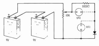
Fig. 3-5. The hookup for drawing a characteristic curve for a diode.
You can run a curve on zener diodes and on small-signal diodes using the simple setup of Fig. 3-5. The finished curve will look some thing like that in Fig. 3-1. That part of the curve to the right of the vertical current line is made with the battery polarity applying positive voltage to the anode of the diode under test. To complete the curve to the left of the vertical line, reverse the battery polarity. The schematic shows a 1000-ohm series limiting resistor to protect the diode against excessive current which might destroy it. You can either use a volt-meter to read the voltage drop across this resistor and convert to current (I= E/R), or connect a milliammeter in series. Make a chart of current versus voltage as you turn the potentiometer up, then transfer the points to a graph. Reverse the battery polarity and plot a similar curve. Reverse current will be extremely low as you go up in voltage in the negative direction, until you reach a point where the current will suddenly take a jump. This is the avalanche point. It establishes the maximum inverse voltage you should safely apply to a diode (except zeners).
Zener diodes are specially designed to run continuously at the avalanche point. The zener voltage-regulating rating is the voltage reached at the point of avalanche. As you increase voltage beyond this point, only the current will increase; the voltage across the diode will remain constant. This is what makes zener diodes good regulators.
Fig. 3-6. A constant output voltage at the zener diode rating is the feature
of this power-supply circuit.
Fig. 3-6 shows a simple low-voltage power supply with a zener diode rated at 8 volts across the output. The voltage to the diode may vary due to fluctuations in the AC line voltage, but the voltage across the diode will always be 8 volts. The current through the diode will increase or decrease with voltage fluctuations preceding it.
For measuring zener diodes with a higher than 8-volt rating, you will need a higher-voltage supply, of course.
TRANSISTOR MEASUREMENTS
Instruments for measuring the standard bipolar transistor vary from a simple go/no-go type (a simple one you can build yourself is described at the end of this section) to laboratory types with high frequency oscillators built in. The most popular instruments make leakage tests and measure DC alpha or beta, which is considered sufficient to check out transistor quality.
To determine what it is that is important in transistor specs, it is necessary to review the meaning of the specs, or at least those in which hams would be interested, and on which they might be able to make some measurements. The data sheets and transistor manuals are full of spec symbols each of which has a specific meaning. There are over a hundred symbols, but only a few are significant to the amateur. Most symbols are almost self-explanatory. Here are a few of the important ones:
V_cbo
Volts between collector and base with the remaining element (emitter) open. The first two letters of the subscript may be any two of the three elements of a transistor, and if followed by an O means the third element is open. If the last letter is an R, it means a resistor of specified value is connected between the remaining element and the second letter subscript. If the last letter is S it means shorted, etc. for other letters.
I_C
Collector current, usually in milliamperes.
h_FE
Forward-current or static transfer ratio for a common emitter configuration. It is also known as DC beta.
DC beta, or h_FE =Ic/Ib
The ratio will vary with different values of collector current, and with temperature. Spec sheets usually show a minimum figure.
h_fe
Small signal forward-current transfer ratio, with AC output short-circuited. It is the ratio of a small change in collector current to a small change in base current. The purpose of the small change is to keep it on the linear portion of the curve. At low audio frequencies the h_fe is often the same as the h FK, but is lower at higher frequencies. Spec sheets frequently give the figures for two frequencies; for example, at 1 kHz and at 20 MHz.
f_1
Gain-bandwidth product frequency at which hfe is unity. It is the highest frequency at which there is no further amplification.
Alpha (a) is the ratio of collector current to emitter current for a common-base circuit configuration, and beta (ß) is the ratio of collector current to base current, usually in a common-emitter configuration.
The two ratios are related, as follows:
alpha = ß / 1 + ß
and
Beta = alpha / 1-alpha
COLLECTOR CHARACTERISTICS CURVE
Probably the most important graphical presentation of the operating characteristics of a transistor is in the collector-characteristics graph, which plots collector volts against collector current for various base currents. The graph for a typical amplifier transistor looks like Fig. 3-7. From it, both DC and AC beta (h_fe and h_ie) can be determined.
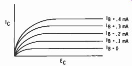
Fig. 3-7. With the setup shown in Fig. 3-8, you can run transistor characteristic
curves, which look like this.
With simple equipment you can run your own set of collector-characteristics curves.
Fig. 3-8 is a schematic of a circuit using inexpensive batteries for the base and collector power sources-10,000-ohm potentiometers are used for adjusting battery voltages. While separate meters are shown in each circuit (for measuring base current, collector current, and collector voltage), a single sensitive VOM could be used by switching it around from place to place. A voltmeter could be used to measure base current by measuring the voltage across the 1000-ohm base-limiting resistor and using Ohm's law (I = E/R). Adjust the base voltage for 0.5 mA and plot collector current for each 5-volt change in collector voltage. Move the base voltage up to 1 mA base current and plot another curve of collector current versus collector voltage. Draw additional curves for increased values of base current.
The final set of curves may look something like Fig. 3-7. Small-signal transistors may require making the base-current increments in micro amperes, not exceeding 1 mA. This set of curves will tell you about all you need to know about the amplifier characteristics of an unknown transistor, except its high-frequency response.
Fig. 3-9 is the hookup for observing the collector characteristics on an oscilloscope. The low-voltage half-wave power supply supplies ...
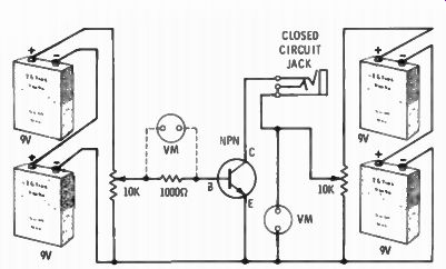
Fig. 3-8. A simple setup for running transistor characteristic curves.
... an AC voltage superimposed on a DC voltage. The horizontal sweep is carried across the CRT during the forward conduction of the rectifier ...
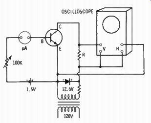
Fig. 3-9. With
a hookup like this, a continuous curve of transistor collector characteristics
can be observed on an oscilloscope. The curve will be different for each
value of base current.
... diode. The trace returns to the beginning during the second half of the wave when there is no voltage. At the same time the pulsating DC voltage is applied to the collector through a load resistor. The vertical deflection on the scope is from the AC voltage across the load resistor. The value of R should be as low as possible and still provide full-scale vertical deflection. The more sensitive the vertical amplifier of the scope is, the lower the value of R can be.
Observe the trace on the scope with each change in current in the base circuit. The meter in series with the base circuit can be a micro-ammeter or a milliameter, depending on the transistor under test. By taping a piece of translucent paper over the face of the CRT, you can trace the curves for each of the settings of base current. It will look something like Fig. 3-10.
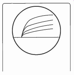
Fig. 3-10. Place a piece of translucent paper over the face of the CRT of
Fig. 3-9. Trace each curve for each change of base current. The final tracing
will look something like this.
FIELD-EFFECT TRANSISTORS
The transistors we have been talking about are called bipolar transistors because their operation depends on the movement of both electrons and holes in the material. A more recent development, and one that is more important to the amateur, is the unipolar transistor, called FET (field effect transistor). Some FET's operate on the movement of electrons, some on the movement of holes, but not both.
The FET has characteristics very much like the vacuum tube. Its input (the terminal is called gate instead of base) has very high impedance. It does not load down an input resonant circuit as does the conventional bipolar transistor, and it, therefore, makes an excellent r-f amplifier.
Tests and measurements on the FET depend on the type. Most FET's are of the depletion type. In them a slab of N-type silicon is connected between the drain and source (so-called instead of collector and emitter) on each side of which is a glob of P-type material connected to the gate. With no voltage on the gate, current will flow in the drain-source circuit if a voltage is applied. As a negative bias is applied to the gate, electron depletion occurs around the P-type material resulting in a constriction in the flow of current from drain to source. As bias is increased, a point is reached at which no current flows in the drain-source circuit. This is the cutoff point similar to vacuum tubes (Fig. 3-11). Some FET'S are enhancement type, with exactly the opposite effect.
Current does not flow in the drain-source circuit until a bias is applied.
Some FET's are called enhancement/depletion type in which some current flows in the drain-source circuit with no bias, and current is increased or decreased by the application of bias, either negative or positive. Most FET's are the earlier mentioned, depletion type.
The all important drain-source current characteristic chart or graph will show drain-source current versus voltage plotted against gate-difference voltages (instead of current) and will look like Fig. 3-12. The method of measurement is similar to that of the bipolar transistor, ...
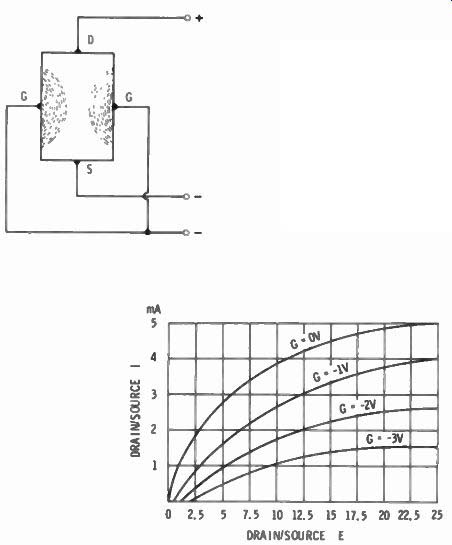
Fig. 3-11. As bias voltage to the gate of a FET is increased, the area around
the gate becomes more and more depleted of electrons. The resulting constriction
is the control of current through the transistor.
Fig. 3-12. The drain/source characteristic curves for a FET transistor.
... except for a voltmeter across the input voltage source instead of a milliammeter. The circuit of Fig 3-18 is easy to put together for the measurement.
Begin measurements by setting all voltages to 0. Plot the figures of drain voltage versus drain current for small increments of drain volt ages from 0 to maximum with the gate voltage at 0. Depending on the transistor, saturation may flatten out the curve as you go up in voltage.
If it does not, be sure you do not exceed the maximum rated current and voltage listed in the transistor manual. Turn the gate voltage up to - 1 and plot another curve under conditions of - 1-volt bias. It will fall somewhere below the curve for 0 bias. Draw additional curves with increased bias voltage. At one bias-voltage point there will be no, or very little, drain current, regardless of drain voltage. This is the cutoff bias.
HANDLING FETS
One of the most important points to remember in testing a FET is the handling. You may have noticed that when you buy a FET it comes with the leads twisted together or wrapped in a metallic foil.
The leads are shorted together to prevent a static charge from accumulating on the gate. The gate P-material is insulated from the N-type slab of the drain-source circuit by an oxide coating which acts as an insulator. This is one of the important factors which gives the gate such high-impedance characteristics. The metallic oxide coating is very thin, and static charge accumulation on the gate could puncture the thin coating and make the FET inoperative. Even the static charge of the human body, if you pick up a FET by the gate lead and touch the drain or source lead to ground, may be enough to puncture the coating.
A TRANSISTOR TESTER
The instrument shown in Fig. 3-13 is home constructed. Anyone can build one. It is a tester of small-signal type transistors to show, to a limited degree, whether they are good or bad.
This tester will indicate the presence of excessive leakage between the collector and emitter, and it will indicate the forward-current transfer quality. While it does not provide the actual figure for DC beta (h_FE ) you can determine whether one transistor has more DC forward gain than another. It will determine whether the transistor is NPN or PNP if this is not already known. The universal-type sockets will accommodate the TO-5 type transistors with leads in a ...
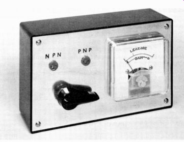
Fig. 3-13. A home-made small-signal transistor tester. It shows relative leakage
and static direct-current gain.
... semicircle, or the flat-type transistors with leads in line. More important than anything else, the cost to build it is small.
In Fig. 3-14 you will recognize the simplest of amplifier circuits, with the base-bias resistor returned to the collector. This provides some positive (+) bias for the NPN transistor. The 390 K resistor limits the base current to a few microamperes. While a lower value resistor here will give a better deflection of the meter, any transistor under test must be protected against damage by the instrument. The deflection is adequate, and all transistors arc fully protected.
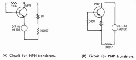
(A) Circuit for NPN transistors. (B) Circuit for PNP transistors.
Fig. 3-14. The fundamental circuit of the tester is shown here in two parts. In the actual unit, polarities are switched.
Fig. 14B is adapted for use with PNP transistors. The 390K resistor is returned to the negative ( -) side of the battery for biasing, and the collector-to-emitter polarity is reversed.
Any 3-ma meter movement, even the cheapest you can buy, will do for an indicator in the collector-to-emitter circuit. A 9-volt battery, of the type found in so many transistor radio sets, provides more than enough current for about any of the small transistors.
The 3000-ohm resistor is subject to change, depending on the meter movement you use. The resistor value to choose is that which, when a short is applied between the collector and emitter terminals of the socket, the meter will just read full scale. You can determine this by Ohm's law or by trial. The Ohm's law formula is:
R=E/I
If E is 9 volts and I is 3 ma (or .003 amp), substituting,
R=3000
The resistance of the meter movement must be deducted from the figure of 3000 ohms. Inexpensive meter movements may have several hundred ohms of resistance. If, for example, the resistance of the meter alone is 700 ohms, the series resistor will be 3000 700 or 2300 ohms. The meter movement used in the instrument shown in these photos had a resistance of 50 ohms (this one just happened to be handy). The 50-ohm resistance was negligible compared to the total resistance so was not figured in the calculations. A total resistance of slightly more than the 3000 ohms, merely means slightly less deflection in gain tests. Even a 10-percent error is not important to the function of this instrument.
The trial method of selecting the collector limiting resistor is to place a 3000-ohm variable resistor in the circuit and, with a short between collector and emitter, adjust the variable resistor for full scale deflection. Then measure the value with a VOM and replace the variable resistor with one of fixed value, or the nearest standard value. You can, however, leave the variable resistor in the circuit; in fact, the variable resistor allows you to make adjustments later to bring the indication up to full scale, as the battery voltage drops from use or age.
The complete circuit is shown in Fig. 3-15. To reduce switching complexity, separate sockets are used for NPN and PNP transistors.
The only switch in the circuit is used to provide bias of the correct ...
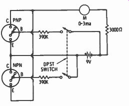
Fig. 3-15. The complete circuit diagram. The switches shown are parts of one
double-pole single-throw (dpst) switch.
... polarity to the base of the transistor for gain measured. With the switch down, the meter reads forward-current gain.
Basic construction is on the panel of a small inexpensive meter case. You may build your tester any way you wish, but complete enclosure in a case, as shown, makes a neat compact instrument.
Parts placement and wiring are not critical as to layout, and any arrangement of sockets, meter, and switch will do. The method shown here is simple and inexpensive (Fig. 3-16). Before you do any cutting you will need to have the parts on hand. Different meters require different sized holes for mounting them on the front panel.
Besides the meter case, panel, and the hardware, you will need:
1, 0-3 ma DC meter, any quality and any size.
1, 9-volt battery (Neda 1604).
1, dpst (double-pole, single-throw), spring-return switch.
2, universal transistor sockets.
1, 2-terminal wiring tie-point.
1, 390.000-ohm, 16-watt resistor.
1, 3000-ohm, 16-watt resistor.
1, snap-on battery connector.
The small panel for the two sockets is 6" X 3.5". The sockets arc mounted on the front panel.
Follow the layout shown in the back view if you wish. A bracket for holding down the battery is bent from a thin sheet of metal fastened to one of the meter-mounting screws, but any method you devise will do.
The meter scale is home made, as can be seen from the photo (Fig. 3-17). The original scale showing 0-1-2-3 in milliamperes may be used as well. To make your own like this requires removal of the case from the meter, and careful handling to prevent damage to the needle and internal mechanism. With the case off, measure the diameter of the scale on the meter, and draw a circle of the same size on a blank sheet of paper. Estimate the arc made by the needle and draw an arc on the new scale. Put in the markings shown. Cut out the new scale, and cut off the lower 1/3 of the circle. Apply rubber cement to the back and carefully slide the new scale under the needle and press it down against the present scale on the meter movement. You may have to cut a small semicircle out of the lower part of the scale to keep from interfering with the movement of the needle. Determine this before you apply the rubber cement, by trying it in place. The PNP and NPN markings on the panel were made from transfer type covered by a coat of clear-plastic spray.
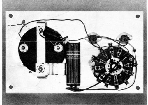
Fig. 3-16. Rear view of the transistor tester showing simplicity.
The transistor sockets are available with mounting flanges or for ring mounting. This model used ring mounting. A 11/32-inch hole was a good friction fit for the sockets without the need for the rings.
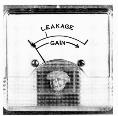
Fig. 3-17. Closeup of the home-made meter scale.
The four holes provide for the insertion of the two common types of transistors. The three holes in a semicircle are for TO-5 type transistors. The in-line holes are for in-line transistor leads, with the two holes at the ends common to collector and emitter for both lead styles. The one close to the emitter hole is base, and is wired to the other base terminal.
All connections, except to the meter posts, are by soldering. Use a resin-core solder only, and a well-tinned soldering iron. One of the small pencil-type irons rated from 23.5 to 40 watts is ideal. Any size up to 100 watts will do, however. Hold the hot iron to the terminal to be soldered for the count of three, then apply the solder. Just a small amount of solder should flow into the crevices of the connection, then remove the iron, and wait until the connection has cooled before disturbing it.
You can purchase snap-on connectors for the battery, but since the battery will last for a long time, solder connections to the terminals can be used if you so desire. It will be a long time before replacement becomes necessary.
USING THE TESTER
If the transistor is a PNP type in a TO-5 case or a similar one, with the three leads in a semicircle, insert the leads into the three outermost holes of the PNP socket. Be sure the leads are gripped by the metal terminals inside. Try pulling gently on the leads. If the transistor is a silicon transistor you may get no or very little deflection before you press the switch. Any movement at this point up scale indicates leakage between collector and emitter. Germanium transistors may show about 14-scale movement upward, and this may be normal. Pressing the switch puts forward bias on the base of the transistor and the needle should move upward, about 14 scale.
Any deflection higher than the leakage deflection means the transistor is in working condition. If there is no movement upward, try the transistor in the other socket, as it may be incorrectly identified. An NPN transistor in the PNP socket will show no deflection, and vice versa.
If the needle goes to full scale when the transistor is first inserted, the transistor is shorted and should be discarded.
This instrument is for checking small-signal NPN and PNP transistors only; it is not for checking FET (field-effect transistor) or UJT (unijunction transistor) types. Both of these types will show what appears to be high leakage when first inserted into their sockets, and this is normal. The FET will show a slight drop in deflection when the switch is depressed. The UJT will show no change when the switch is pressed.
TRANSISTOR MANUALS
In addition to individual spec sheets on transistors, the principal manufacturers also produce complete manuals on their line of transistors. Complete specifications are shown, and general data and typical circuits are frequently included. These are available at your electronic parts dealer. Perhaps the most complete listing of all transistors is the Howard W. Sams "Transistor Specifications Manual."