Sections 2, 3 and 4 provided basic outlines of various aspects of the CD player aimed generally at block diagram level to enable a fundamental appreciation to be achieved.
This section is intended to provide an understanding of a wide range or circuits at circuit diagram level since many players of differing manufacture tend to utilize a common selection of Sony and Philips integrated circuits which are used for the RF processing, servo operation and decoding circuits, and this will prove useful as a basis of understanding for the majority of circuits used within most CD players.
Over the years the CD player has in many ways remained the same from one generation to another. The circuitry has evolved from a wide range of discrete components in the early players to just a few integrated circuits in the more recent models. However, the overall operation of the different players has remained relatively similar, and therefore a reasonable understanding of a range of selected circuits will generally enable a reasonable appreciation of many CD players to be achieved.
The following circuit descriptions are based on a group of integrated circuits (ICs) which provide the RF amplifier, servo control and signal decoding functions. There have been various generations of each group of these ICs, as indicated below, but experience has shown that there are similarities in their operation when comparing each generation, and that it is the new technologies as they have been developed which may have evolved the ICs into apparently much more complex packages.
Author's note:
Reference to specific component identifications, such as resistors, capacitors, transistors, and especially photo-diodes (i.e. A, B, C or D), may appear at variance to relevant circuit diagrams. Wherever possible it has been the author's intention to maintain consistency throughout this guide to ensure cross referencing is as accurate as possible, and he apologizes for any unintended errors that may 'slip through'.
Sony types (three generations)
RF Amplifier Servo control Decoder
CX20109 CX20108 CX23035 CXA1081 CXA1082 CXD1125 or CXD1135 CXA1471 CXA1372 CXD2500
Some later Pioneer and Sony players have a small sub-board fitted onto the optical assembly which has an IC that replaces the CXA1471, and may be identified as the M51593FP on Pioneer players, or the M52103FP on Sony players.
Philips types (three generations)
Photo-diode Radial error
Decoder processor processor
TDA5708 TDA5709 SAA7010/ SAA7020 TDA8808 TDA8809 SAA7210 TDA8808 TDA8809 SAA7310
Concerning the RF and servo processing circuits, there are many similarities in their general overall operation, and their various generations contain improvements in package density, circuit efficiencies in the areas of circuit processing techniques, and the voltage, current and temperature handling characteristics. It is the decoder circuits that have evolved more radically with more complex error correction, with the Sony CXD2500 having the RAM included internally, whilst many other decoders maintain the RAM externally. The latest Sony decoder to arrive on the scene (mid-1993) is the CXD2515, which combines not only all the decoder functions, including the RAM, but also the servo control, which operates digitally to provide automatic servo correction and gain control of the focus and tracking servos.
With this form of decoder, and similarly to the players using the Toshiba TC9220 and TC9221, servo and decoder ICs which provide automatic circuit control, many players will now have Virtually no adjustments, with the possible exception
SAA7010/ SAA7020 SAA7210 SAA7310
Concerning the RF and servo processing circuits, there are many similar it ies in their general overall operation, and their various generations contain improvement s in package density, circuit efficiencies in the areas of circuit processing techniques, and the voltage, current and temperature handling characteristics. It is the decoder circuit s that have evolved more radically with more complex error correction, with the Sony CXD2500 having the RAM included internally, whilst many other decoders maintain the RAM externally. The latest Sony decoder to arrive on the scene (mid-1993) is the CXD2515, which combines not only all the decoder functions, including the RAM, but also the servo control, which operates digitally to provide automatic servo correction and gain control of the focus and tracking servos.
With this form of decoder , and similarly to the players using the Toshiba TC9220 and TC9221, servo and decoder ICs which provide automatic circuit control, many players will now have virtually no adjustment s, with the possible exception of a couple of mechanical radial/tangential adjustments to ensure optimum operation of the optical block.
With respect to players that utilize the Sony type circuits, the combinations of the CXA1081/ CXA1082 and CXA1471/CXA1372 generally provide the same overall functions. Therefore their relevant circuit operations will be generally similar, and the CXA1081/CXA1082 combinationwill be used for the actual circuit descriptions, with any additional information included as necessary.
But it is worth noting that the CXA1372 does contain some elements of the circuits used in the CXAIUul, in particular the circuitry after the RF input (RFI) pin 1 as well as the servo control of the CXA1082.
The CXA1471 is generally a photo-diode processing RF amplifier, providing only the RF, focus error (FE) and tracking error (TE) signals.
Some 1992 Pioneer and Sony players utilize a small sub-board attached to the optical assembly, with a small RF integrated circuit, either the M51593FP or the M52103FP producing these three signals direct to the CXA1372 as relevant.
With regard to circuits using the Philips ICs, the TDA8808/TDA8809 will be referred to as necessary, because of the widely differing circuit techniques that exist between players that use either the Sony or Philips type ICs.
Whilst players of other manufacture may appear to use totally different ICs, some are, in fact, similar under a different identification. It is the general circuit description that is intended to be applied to the majority of circuits that engineers will encounter.
Photo-diode array and RF amplifier stages
Philips circuit: photo-diode signal processor TDA8808
With reference to Fig. 5.1, the four photo-diodes, D17D4, are connected to pins 22-25 of the photodiode signal processor, TDA8808, and from these diodes will be formed the focus and radial tracking error signals. Also the sum of the four diodes, together with the guard ring photo-diode, are applied to pin 26, HF In, to eventually produce the RF eye pattern signal.
The signals derived from D1, D2, D3 and D4 are each amplified by gain controlled amplifiers, before being filtered and added together in pairs (D1 + D2) and (D3 + D4) to provide the two radial error signals RBI and RE2. These two signals are also added together and fed to a gain control stage to provide an output for controlling the gain of the four diode input amplifiers.
The HF In signal at pin 26 is amplified and passed through an equalizer stage to provide the RF eye pattern signal output, HF Out, at pin 3.
The inclusion of the guard ring photo-diode, together with the four main photo-diodes, enables this type of optical assembly, which is of the single-beam type, to compensate for any scratches or other possible problems on the playing surface of the disc.
Whilst the HF Out at pin 3 is passed to the decoder it is also fed back to pin 4 to be applied to the HF amplitude slicers and then in turn to the gain control circuit.
Four individual diode outputs, 1, 2, 3 and 4, appear after each filter, and are passed to the focus normalizing circuit, to provide the focus error (FE) signal at pin 15.
At pin 6, communications from the system controller are fed to the starting circuit to switch on the laser diode, as well as commencing the focus search sequence in the focus normalizing circuit.
The laser on (L0) output from the laser supply at pin 17 will go high to switch on transistor 6502 and in turn the laser diode. Stabilization of the laser diode light intensity is maintained from the monitor diode by being applied via pin 18 to the laser supply circuit.
Laser power is controlled by the preset 3520 which varies the working point at pin 18.
Sony CXA1081S RF amplifier:
photo-diode input
The integrated circuit shown in Fig. 5.2 appears in many players, and the general principles of operation can be applied to earlier, and even later, circuits that fulfilled these functions, as well as very similar versions occasionally identified under different type numbers.
Figure 5.1 Philips circuit--photo-diode signal processor TDA8808
Laser power control
When the LDON signal from the system control applied to pin 29 is LOW, the output at pin 5
Figure 5.2 Laser automatic power control (APC) circuit will also go LOW
allowing transistor Q1 to conduct, switching on the laser diode. The monitor
diode MD passes to pin 6 a measurement of the light intensity from the
laser diode which enables the automatic power control circuit (APC) formed
by the two internal op-amps to maintain a stabilized laser diode output.
VR1 provides the operating point for the circuit via pin 6 to determine the necessary laser intensity from the laser diode.
RF amplifier circuit (Fig. 5.3)
The output from the photo-diodes is initially amplified before being applied as two pairs of signals (A + D) and (B + C) to pins 7 and 8 as PD1 and PD2, where they are further amplified before being summed together in the RF summing amplifier to provide (A + B + C + D), which will become the RF eye pattern signal (RFO) at pin 2.
A certain variation occurred in some Pioneer players with the introduction of a delay line in the preceding photo-diode circuits, as illustrated in Fig. 5.4.
Accu-focus system
The purpose of the delay lines is to minimize any signal distortion that may occur because in effect the 'pits' from the disc will reach the preceding photo-diodes A and B first, and provide an output which will be fractionally ahead of the outputs from C and D, which may appear to develop an inconsistency in the quality of the total output signals. Though this method may have had advantages in reducing distortion and noise, together with a more accurate type of signal, it was however a system that was not continuously maintained throughout all the models that use this particular type of IC.
Focus error amplifier
Within the IC shown in Fig. 5.5 the two internal signals VA and VB, which are the result of the opposite connected diode pairs (A + D) = VA and (B + C) = VB, are applied to the focus error amplifier to provide the focus error signal (FE) output at pin 19.
The FE bias control connected to pin 18 is usually identified as the focus offset control in many players, and is a potential which is variable usually between Vcc (+ 5 V) and Vee (5 V) to
Figure 5.3 Sony CXA1081S RF amplifier -- photo-diode input neutralize
any undesirable d.c. offset potentials with the focus servo system.
Focus OK circuit
When the CD player is operated after a disc has been inserted, it is necessary for a particular sequence of logical events to take place before complete playing of the disc can commence. These are usually as follows:
1 laser on: difficult to focus in the dark;
2 focus search: to detect that a disc is present, and enable focus to be achieved;
3 rotate the disc: enable the disc to reach roughly the correct speed; and
4 switch on the tracking servo: sequence complete and disc now playing.
Some variation in this sequence may occur in relation to when the disc commences rotation, with some manufacturers enabling the disc to rotate before the focus operation.
After switching on the laser and the focus search sequence taking place, the RFC signal from the RF summing amplifier is fed to one side of the focus OK amplifier, and then from pin 2 Via a capacitor to pin 1 to the other side of the amplifier. At the correct focal point the RF signal will be at a maximum level, which will enable a high level to be obtained at the F-OK output at pin 28.
This FOK signal is passed to the system controller to inform it that a disc is present and that focus has been achieved, enabling the next relevant sequence to take place (Fig. 5.6).
Tracking error amplifier
With the common three-beam optical assembly, two photo-diodes (E and F in Fig. 5.7) are used for the purpose of developing the tracking error signal. The signals from these two diodes, after initial amplification, are applied to pins 10 and 11, for further amplification. The outputs from this stage of amplification are now passed to a differential amplifier, to provide the tracking error (TE) signal at pin 20 (Fig. 5.7).
Figure 5.4 Accufocus system
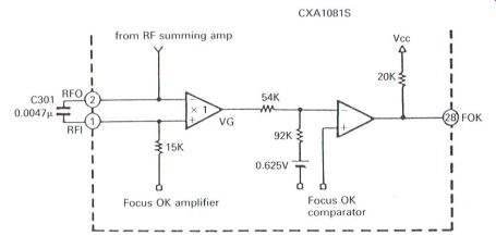
Figure 5.6 Focus OK circuit
The signal output at this pin will be a potential, the value and polarity of which will be related to the amount and direction of tracking error.
It is essential when an error occurs to one side of the track, which will produce a potential of a specific level and polarity, that an equal error on the other side of the track enables a level to be produced that is equal in amplitude, but opposite in polarity. For this to be achieved, the gain of one of the input amplifiers can be adjusted. Connected between pins 12 and 13 is the tracking balance control identified in Fig. 5.7 as VR5.
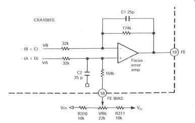
Figure 5.5 Focus error amplifier
Mirror circuit (Fig. 5.8)
It is essential that the laser beam effectively follows the track on the disc. However, it is possible for the beam to follow the space between the tracks, and to ensure this does not occur continual monitoring of the RF signal is maintained. If the beam was tracking between tracks, the reflected beam would be maintained at a consistently high level, and this level would be used to 'inform' the system control and tracking servo to 'kick' the beam onto the track.
The RF input (RF1) to pin 1 is in fact the eye pattern waveform (RFO) monitored with the oscilloscope timebase operating at a relatively low speed to compress the waveform as shown, and will fluctuate either side of 0 V due to the capacitor C1. The waveform illustrated shows the RF Circuit descriptions signal building up to a maximum level as the laser locks onto the track correctly.
The signal is amplified to provide the inverted signal at (G), with the upper peaks of this waveform relating to 'on-track' conditions, and the troughs being related to almost 'off-track' conditions.
Further processing of the signal through the peak and bottom hold circuits will now develop the signals (H) and (I), that relate to the average of each of the signals above and below the 0 V level, and provide the signal (J) from the comparator section.
This signal is now applied to the mirror hold amplifier, where the level (K) is developed in relation to the hold capacitor at pin 23, and the mirror comparator where the combined effect of the signals (J) and (K) produces a series of high and lows that relate to the off-track (high) and on-track (low) conditions.
EFM comparator
The RF eye pattern waveform (RFI) is derived from pin 2 and applied to pin 1 via a capacitor.
The effective aim is to turn the signals which consist of a series of amplitude variations (depending upon the lengths of the pits and spaces) that are being retrieved from the disc, and turn them into a series of square waves. However, it is necessary to consider the possibility of asymmetry caused during the manufacture of the disc, where the quality of the pits or bumps on the disc may not be consistent from one disc to another.
The capacitor connected between pin 2 and pin
Circuit descriptions
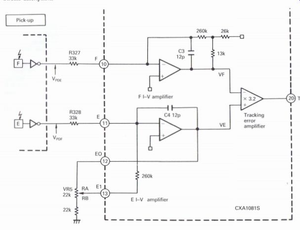
Figure 5.7 --- Tracking error amplifier 1 can help to overcome asymmetry
problems, but further processing is usually necessary.
The output from the EFM comparator (Fig. 5.9) is fed from pin 27, through a buffer stage which is usually within the decoder, and then through a filter back to pin 26 (ASY), where via an internal buffer and amplifier stage it becomes the reference or working point from which the comparator can operate.
Usually 2.5 V will be present at pin 26 which is derived from the decoder (CXD1135) pin 6.
The EFM comparator comprises a dc loop from pin 27, through the buffer in the decoder to pin 26 and via the internal ASY buffer and amplifier stages back to the EFM comparator. The RF eye pattern input to pin 1 appears at pin 27 as square waves, but the leading and lagging edges of the waveform (which are in fact the 1's information of the digital data) can be affected by the quality of the 'pits' or 'bumps' on the disc, Fig. 5.10.
The filter between pin 6 of the decoder and pin 26 will remove the square wave variations, to develop a slight variation of the nominal 2.5 V at pin 26 due to the charge developed by C316.
This resultant potential will be related to the disc quality, which in turn is passed to the EFM comparator to ensure that a high quality of square waves is maintained for further processing in the decoder.
The filter will cause C316 to charge up, or integrate the signal, to the mid-point level of the maximum and minimum levels, to provide the previously mentioned reference or working point, and become an automatically variable level, auto asymmetry, which is related to the pit quality of each disc as it is played.
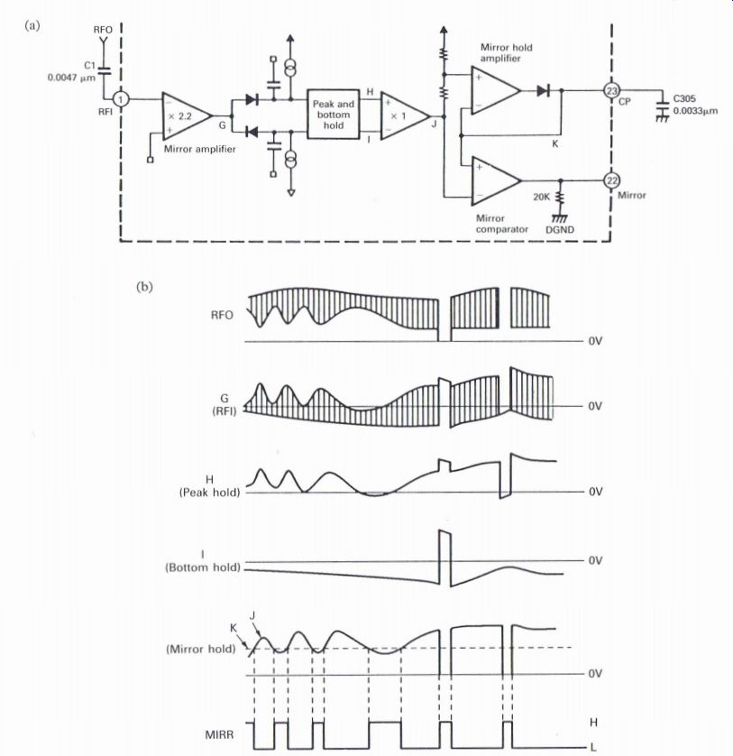
Figure 5.8 Mirror circuit; (a) circuit (17) waveforms.
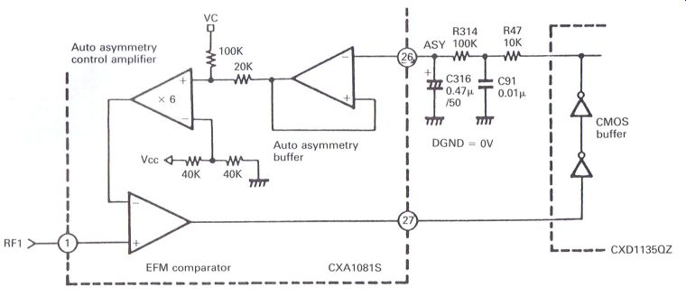
Figure 5.9 EFM comparator
Defect circuit (Fig. 5.11)
It is essential that when a defective disc (i.e. with scratches) is played some form of damping occurs within the tracking servo circuit; otherwise it is possible for track jumping to occur when scratches pass through the laser beam.
The RF eye pattern waveform (RFO) at pin 2, (a), is inverted at the output of the defect amplifier, waveform (b), which becomes the bottom hold signal. As the effect of the scratch now appears positive going both of the diodes, D1 and D2, will be prevented from conducting for the period of the positive going scratch pulse.
During periods when no major scratches are present, both D1 and D2 will slightly conduct as a result of point (b) being low, and a current flowing from both the positive current references and capacitor CB will be charged slightly positively. When scratches occur D1 and D2 will stop conducting.
As a result of D1 not conducting, the positive current reference will now appear at pin 16 (CC1) and is coupled Via the capacitor, CC1 to pin 15 (CC2), causing the pulse to appear at (c) which is applied to the positive input of the defect comparator.
When D2 is prevented from conducting, CB will commence to charge up more positively, but due to the short duration of the first or small scratch pulse this will not cause any increase of the level occurring at pin 24. As a result, a short duration square pulse (e) will appear at pin 21 (defect).
For a more excessive scratch, CB will be able to charge up more positively, as shown on the dotted line for the signal (d), and the longer square pulse at (e) will terminate when the level at ((1) becomes greater than that at (c), causing the comparator output to change over. This is to ensure that there is a maximum allowable defect pulse length of 1.4 ms to occur for scratches that are of a longer duration; 1.4 ms is equivalent to a scratch width of approximately 1 mm.
Philips circuit: radial error processor, TDA8809
The radial error signals from the TDA8808 (Fig. 5.12) are applied Via pins 27 (RB1) and 28 (RE2) to a summing and dividing network to provide a range of outputs for further processing.
Signals (re1) and (re2) from the summing and dividing network each pass to a multiplier, where an input from the offset integrating amplifier is also applied. This input is related to the level of tracking error determined from the detected phase of the wobble frequency.
The second pair of multipliers have an input from the gain integrating amplifier which is the result of comparing the phase of the wobble frequency at 45° and the phase of the returning radial
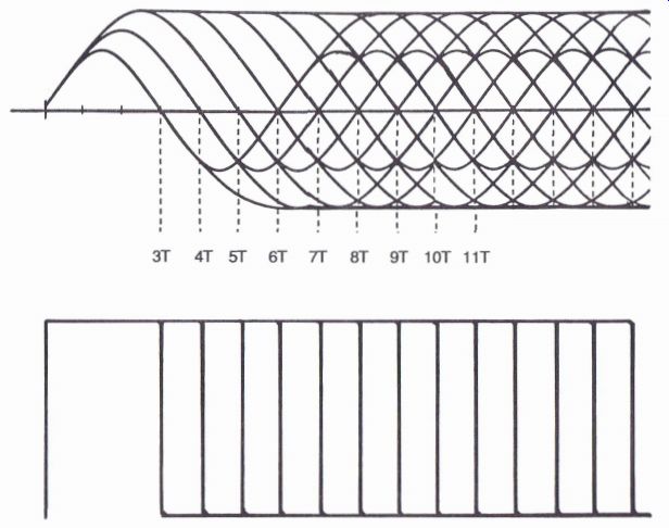
Figure 5.10 Eye pattern and square wave illustrations error signal which
will also contain 650 Hz. The phase relationship will be related to the
quality of the disc reflectivity, laser power and the radial position on
the disc, factors which can affect the overall stability, and therefore
it is possible to achieve a level which can control the gain of the radial
error servo to maintain the necessary stability.
After the multipliers, the two radial error signals (re1) and (re2) pass through a subtractor or comparator to provide the radial error signal (RE), which then passes through the adder where the 650 Hz wobble frequency is injected.
The resultant radial error signal (RE) appears at pin 19 and passes via an anti-skating filter to pin 16 for further amplification to finally appear at pin 15 for application to the radial assembly after final amplification in the radial drive amplifier.
The function decoder receives information from the system controller through pins 8, 9, 10 and 11, which controls the operation of various switches within the IC as well as the 3.5 bit DAC which controls track jumping via the final adder preceding pin 15.
When track jumping occurs, due to selecting another music track or when selecting 'fast forward' or 'reverse', it is necessary to reduce the overall gain of the circuit during this process, and to ensure that the laser beam is directly on track before restoring the circuit back to normal operation. This is achieved by monitoring the (RE dig) signal available at pin 7 (which is related to the
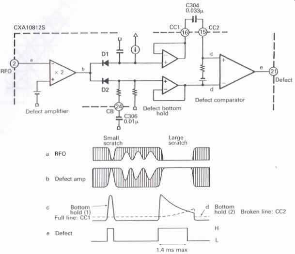
Figure 5.11 Defect circuit position of the laser beam compared to the
track), and feeding this signal to the system controller.
Of the various internal switches which are controlled at various stages of enabling the radial error servo to operate correctly, switch 7 when in the up position feeds the basic radial error signal into the offset circuit at the commencement of playing the disc when 'tracking lock' is being achieved, and then for the fine control the switch will change state to the low position to feed in the detected ()50 Hz phase detected level.
The internal radial switch between pins 16 and 15 will open and close the radial error servo loop to ensure that tracking commences at the correct point. It will also be operated in the test mode to control the servo as necessary.
Sony CXA1082
Focus servo system (Fig. 5.13)
The focus error signal (FE) from pin 19 of the RF amplifier IC is applied via the focus gain control to pin 6 and passed through to the focus phase compensator, which will apply correction to the overall circuit in relation to the specific frequency range within which the focus servo
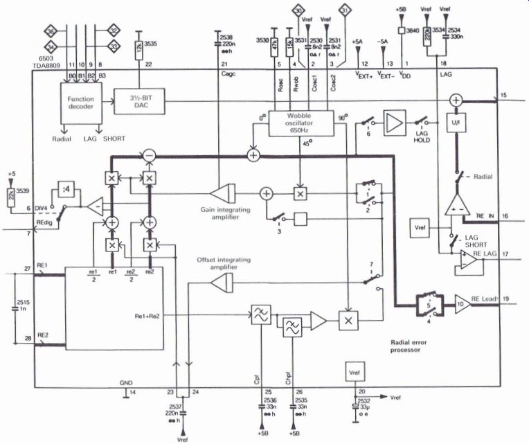
Figure 5.12 Philips circuit: radial error processor YDA8809 operates,
to finally appear as the focus error output (FEO) at pin 11.
A range of switches within the servo 1C are controlled by output from the internal logic circuits, which in turn are controlled by the system controller via a CPU interface circuit which is usually incorporated within the decoder. These switches will control all the required operations of the focus, tracking and carriage servos.
The focus zero cross (FZC) is passed to the internal logic control circuits which, together with the focus OK signal (FOK), will determine the focus opening (F84), and enabling the complete loop to be closed.
The (DEFECT) and (F83) switches reduce the servo gain either when a defect occurs, or in the case of (F33) when focus is operating normally and a lower gain is normally required (compared to a higher gain when focus is initially acquired).
The focus phase compensator output after further amplification is fed from pin 11 to the focus drive circuit and the focus coil to complete the overall circuit. Occasionally a complementary push-pull pair will drive the focus coil instead of the circuit illustrated.
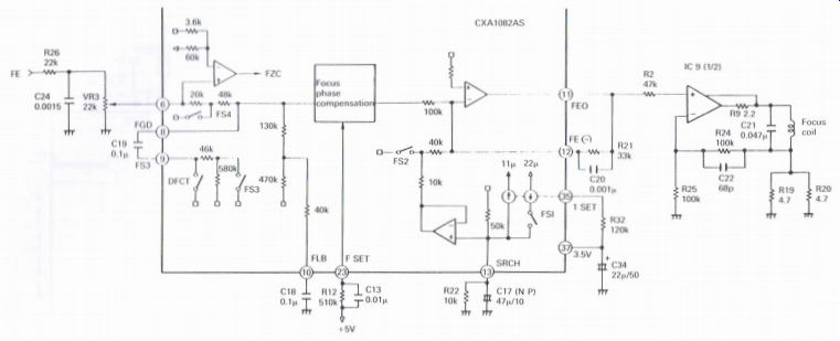
Figure 5.13 Sony CXA1082 focus servo system
A focus return signal developed across the two 4.7 ohm resistors is fed back to the inverting side of the op amp as a focus error rate signal to stabilize the focus servo operation and prevent the focus coil operating erratically as focus errors occur. With circuits that contain the complementary push-pull pair, the focus return signal is usually applied to pin 12.
When a disc is inserted into the player it is necessary for a focus search sequence to take place, by raising and lowering the lens, to enable the correct focal point to be achieved. This is performed by the focus search (F82) and focus up/ down (F81) switches, which, together with the focus open/close (F84) switch, are controlled by the internal logic circuits.
During focus search the sequence of operation is as follows:
F84 will be CLOSED F82 will OPEN F81 will be CLOSED At this point the lens will move to one end of its travel.
When F81 is CLOSED, the current reference of ell 11A and + 22 LIA will provide + 11 11A to flow through the internal 50 K resistor, providing 0.55 V (22 uA + (~11 pA) X 50 K = 0.55 V) to be applied to the input of the internal op-amp and also C17, the search (SRCH) capacitor, which is connected to pin 13. The output from the op-amp will appear, via another internal amplifier, at pin 11, and after feeding through the focus drive amplifier will be applied to the focus coil thus causing the lens to move to one extreme end of its travel.
After a brief period of time (~1 sec), F81 will OPEN removing the + 22 11A internal reference, and now only--11 "A will be applied to the internal op amp and C17. This will enable the lens to move to the other extreme, at a rate controlled by the charge/discharge of C17 as it adjusts to the change in potential. This sequence usually occurs twice if no disc is present or if the laser circuit is defective, and is controlled by data interchange between the system controller and the servo IC.
If a disc is present, and assuming that the laser circuit is operating correctly, only one focus search sequence is necessary as the lens moves through the correct focal point, a maximum reflected signal will be obtained from the surface of the disc, which will result in the focus OK (FOK) signal going HIGH. At the focus zero cross (FZC) point F84 will be opened to switch on or close the focus servo loop, and F82 will be closed to remove any focus search potentials.
An interesting addition to the input of the focus drive circuit can occasionally be observed in some earlier Pioneer multi-disc players, where, typical of these players, the optical block was installed upside down, i.e. with the lens facing downwards, upside down, i.e. with the lens facing downwards, and was therefore subject to gravitational effects.
With the process of selecting each disc from a six-disc magazine, each disc would 'sweep' past the lens, which could have a possible detrimental 'de-capping' effect on the lens as well as causing physical contact between lens and disc surface during certain stages of the operation of selecting and de-selecting the discs.
Focus correction circuit
The effect of the correction circuit (Fig. 5.14) is to feed a residual bias current through the focus coil to raise it into its normally neutral position.
Later models refrained from using this type of circuit, and achieved the raising of the lens to its neutral position by adjusting the focus offset adjustment to a pre-determined level, usually a negative potential, which provided the same compensation.
Tracking and carriage servo circuit (Fig. 5.15)
The tracking error (TE) from pin 20 of the RF amplifier IC, CXA1081, is applied via the tracking gain control to pin 3, which then passes through the circuit to emerge at pin 17 as the tracking amplifier output (TAO).
The tracking error (TE) is also applied via C27 to pin 4 as the TZC signal, to provide the correct time to apply the brake operation to the tracking servo during track jump sequences.
As with the focus servo circuit, various internal switches, which are controlled by outputs from the internal logic circuits, provide the various required control functions for the tracking and carriage circuits.
The two TG1 switches, and TG2, provide the required gain control functions that are needed during the initial track search process. Usually a higher gain is required as tracking is achieved, and a reduced gain when tracking is functioning normally. Also, different gain levels are required during the various track jump sequences.
TM1 switches the tracking servo on (TM1 open) and off (TM1 closed).
TM2 controls the carriage servo in a similar manner to TM1.
TM3 and TM4 provide positive and negative current references for track jump requirements.
TM5 and TM6 operate in a similar manner to provide forward or reverse carriage movement; an extremely useful function in the test mode function to ensure that the carriage servo can be operated when either a high or low can be monitored at pin 20, which should cause the carriage to function.
TM7 provides a smooth brake function to stop further sideways movement of the objective during track search sequences. TM7 will be momentarily closed when the laser beam is precisely on track, a fact that is determined by comparing the mirror (MIRR) input at pin 48, and the TZC signal within the internal logic circuits to provide the specific moment to close TM7 (as shown in Fig. 5.16).
The tracking error (TE) signal at pin 3 passes through the various gain control circuits and the tracking phase compensation circuit (which will provide the necessary frequency correction), to appear at pin 17 to be applied to the tracking drive circuit, which will usually be either a complementary push-pull transistor pair, as shown by Q6 and Q7, or as in many players, an op amp to drive the tracking coil.
The signal applied to the tracking coil is also fed to pin 19 via a filter circuit comprising R50, R51, C39 and C40, which will remove the high frequency tracking error variations, and provide a relatively low frequency d.c. variation, to provide an output at pin 20 (SLO), for operating the carriage or sled motor to move the carriage assembly. As the tracking coil moves the lens across the surface of the disc, it is necessary to gradually move the optical block to compensate for the sideways movement of the objective lens, and ensure that the carriage motor moves the optical assembly before the lens reaches the limit of its travel, which could result in skipping or jumping of the sound.
Disc, spindle or turntable motor servo circuits
-----------------
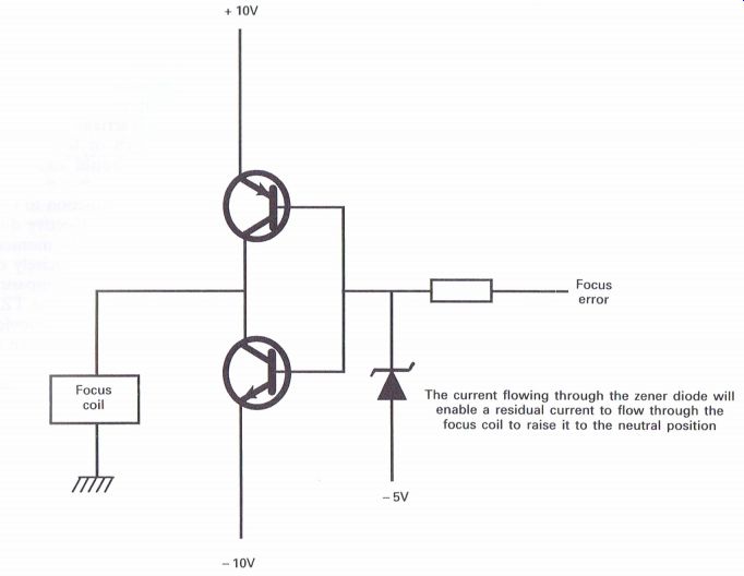
Figure 5.14 Focus correction circuit
The current flowing through the zener diode will enable a residual current to flow through the focus coil to raise it to the neutral position 5V At switch on all three transistors are non-conducting, and the focus coil will be in the low position.
On completion of the reset, the reset input will be high, switching on all three transistors, providing a small residual current through the focus coil to raise it to its neutral position
------------------------
Generally speaking the decoder will provide the actual motor speed information, whilst the system control will provide the relevant motor control information. The motor speed is a function of the data information from the disc, after processing within the decoder, compared with a
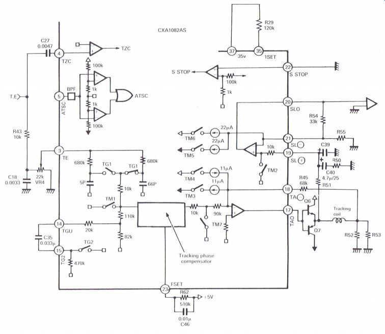
Figure 5.15 crystal source which is also applied to the decoder.
It is necessary to switch on the motor at a pre-determined point, which is a function of the system control circuits. This point is usually dependent upon the manufacturer. The usual sequence is where the disc motor commences operation after the laser and focus have achieved correct operation by ensuring the laser beam is correctly focused onto the playing surface of the disc. An alternative method is to commence rotating the disc just before the laser and focus commence operation to ensure the laser beam can correctly focus onto an already rotating disc, which in some cases may be warped.
Sony CXA10XZ tracking and carriage servo circuit Philips disc/turntable motor servo circuit The circuit shown in Fig. 5.17 provides a useful guide to the operation of a typical circuit used within the Philips based players. Two inputs are provided:
1 MCO--the 'motor control on' signal 2 MCES--the motor speed control signal The motor control on (MCO) signal will be high to switch off transistor 6106 when the laser beam has achieved focus onto the disc. This is achieved when a ready (RD) signal from pin 21 of the
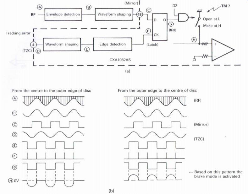
Figure 5.16 (a) Switch TM7 bra/ac circuit and (1)) related signals photo-diode
signal processor (TDA5708) starting circuit, which will be high when focus
has been achieved, is passed to the error correction IC.
(Please refer to the relevant circuit diagram.) Switching off transistor 6106 will in turn switch off transistors 6117 and 6107, enabling the turntable motor control circuit to commence operation. The MCES signal will comprise a 50% duty cycle square wave at a frequency of 88.2 kHz when the player is first switched on or when in standby condition (as shown in Fig. 5.18(a)).
When the turntable is instructed to commence operation, the MCES signal square wave radio will alter as shown in Fig. 5.18(b), and will now have an approximate frequency of 44.7 kHz, and is in fact the disc run-up signal to achieve the correct nominal running speed, which when achieved will change over to the waveform shown in Fig. 5.18(c) during normal play operation. These square wave signals are integrated by resistor 3128 and capacitor 2125 to provide a signal which is processed by the IC6103 A and B. The output from pin 7 of 6103B is fed, via resistor 3116, as Vc, to the turntable brushless motor circuit.
An alternative more simplified circuit (Fig. 5.19) is used to drive the common and conventional small spindle motor, so common in the majority of players.
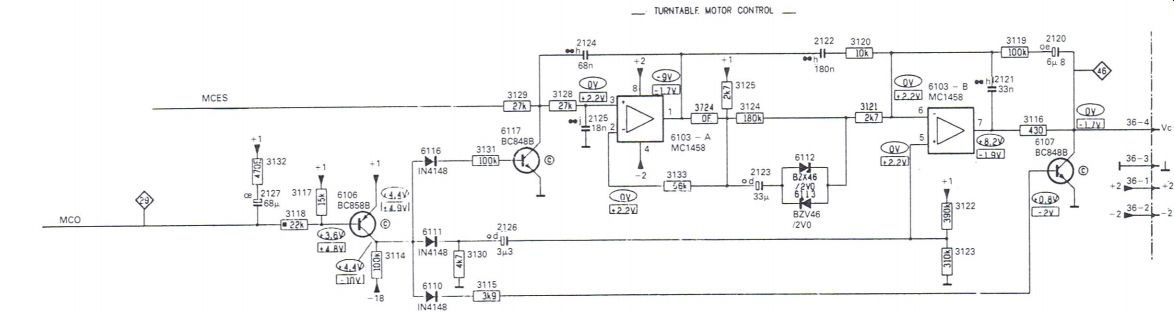
Figure 5.17 Philips disc/ turntable motor servo circuit
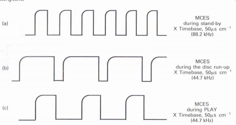
Figure 5.18 Turntable motor control waveforms
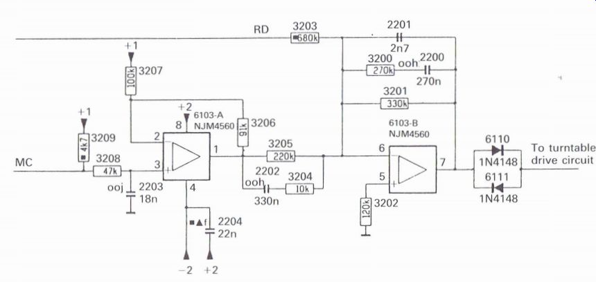
Figure 5.19 Alternative Philips turntable motor circuit
Alternative Philips turntable motor circuit With this circuit again two inputs are provided, which comprise the ready signal (RD) and the motor control signal (MC), which provide an identical function to the MCES signal previously described.
The ready signal, as previously described, will be high when the laser has achieved focus on the playing surface of the disc, and this will switch on the turntable motor control circuit of IC6103B.
The motor control signal (MC) is applied from the decoder to pin 3 of 6103A, via the integrating circuit 3208 and 2303, with the final motor control output, Vc, from pin 7 of 61033, via diodes 6110 and 6111.
Pioneer spindle motor circuit (Fig. 5.20) Four outputs are applied from the decoder, CXD1130 or CXD1135, to the spindle motor
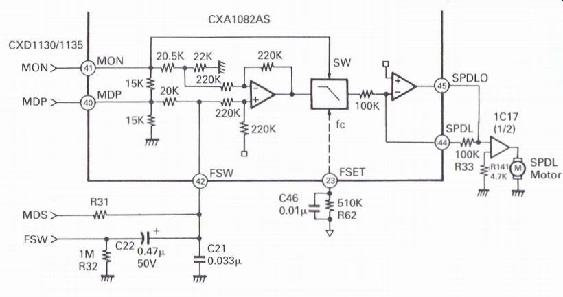
Figure 5.20 Pioneer spindle motor circuit servo circuit contained within
the servo IC, CXA1082.
These are as follows:
1 MON: the motor on or off signal
2 MDS: the motor drive speed or coarse control signal
3 MDP: the motor drive phase or fine control signal
4 FSW: the filter switch signal, to control frequency servo response during coarse and fine operation
A basic description of the spindle motor servo is included in Section 2, with a signal being derived as a result of a comparison between data from the disc and a crystal source; additional relevant information is also included in the decoder circuit description, later in this section.
The basic conditions and waveforms that can be monitored at the MON, MDS, MDP and FSW points are illustrated in Table 5.1 and Figs 5.21 and 5.22.
During the initial run-up of the disc, after the laser and focus circuits have enabled the laser beam to become focused onto the playing surface of the disc, the disc or spindle motor is given a kick start with the application of the MON signal, which will be high, and together with the MDS signal the motor will commence to increase in speed. At this point FSW will be low to introduce C32 at pin 42 to ensure that the circuit will not respond to any high frequency components that may be present.
As the disc runs up to speed the decoder will be 'looking' for the sync. signal and comparing it with the crystal frequency of 8.4672 MHz.
Although the frame sync. signal is referred to as having 24 bits, which comprise a 1 followed by ten 0's, another 1, followed by 10 more 0's and another 1, with a 0 inserted at the ends to ensure that the sync. signal 'slots' into an frame sync. window within the decoder (usually a 23 bit shift register), it is looking for the first 23 bits of the sync. word, which will develop a waveform to equal 22 bits when the disc is running at approximately the correct (rough) speed.
When these 22 bits are compared to 22 cycles...
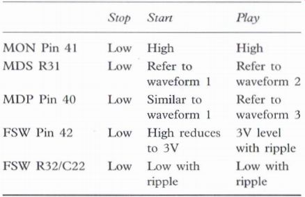
Table 5.1 Spindle motor servo control signals and sequences
Slop Start Play MON Pin 41 Low High, High MDS R31 Low Refer to Refer to waveform l waveform 2 MDP Pin 40 Low Similar to Refer to waveform 1 waveform 3 FSW Pin 42 Low High reduces 3V level to 3V with ripple FSW R32/C22 Low, Low with, Low with ripple, ripple
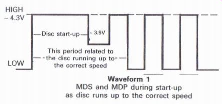
Figure 5.21 Spindle motor servo MDS and MDP signals during disc run-up
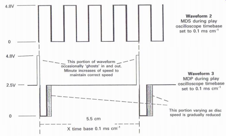
Figure 5.22 Spindle motor servo MDS and MDP signals during play
... of the 8.4672 MHz crystal frequency which is in effect driving the decoder, the disc is considered to be running at approximately the rough or coarse speed.
At this point the tracking servo will be closed, and the MDP signal will now be the result of comparing the data from the disc, which will lock the VCO (see below) to provide an output of 4.3218 MHZ, which after further frequency division, can be compared to an identical frequency which is derived from the 8.4672 MHZ crystal frequency reference.
Comparison of these two frequencies in both frequency (speed/coarse control) and phase (fine control) will develop a combination of MDS and MDP signals to provide the final speed control of the spindle motor.
The FSW signal will be high when the coarse or rough speed has been achieved and the tracking servo is closed, increasing the frequency response of the filter connected to pin 42.
The resultant output at pin 45 is applied to a current driven amplifier stage to finally drive the spindle motor.
A slight variation can occur in this area where the signal from pin 45 is applied to a voltage-
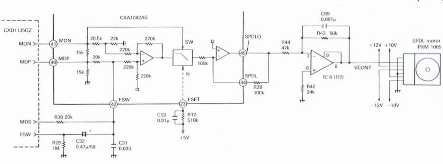
Figure 5-23 Sony CXA1082 focus servo circuit
EFM
To data input processing Phase comparator Loo vco vco timing 4.3213 MHz film? 8 54 MH--generator
(divide by 2)
Figure 5.24 Basic block diagram of VCO/PLL driven amplifier circuit to
drive a brushless spin-le motor (Fig. 5.23).
Voltage-controlled oscillator--phase locked loop circuit
A voltage-controlled oscillator (VCO) is necessary within the CD player to provide a disc data frequency of 4.3218 MHZ for the main purpose of deriving signals for the operation of the disc or spindle motor circuits.
The EFM signal from the disc contains a fundamental data clock frequency of 4.3218 MHZ, which is applied to the phase comparator (Fig. 5.24). Also applied to the phase comparator is 4.3218 MHZ which is derived from the 8.64 MHz VCO after being applied to the VCO timing generator which is in effect a divide by two circuit.
The resultant output from the phase comparator is applied, via the loop filter which will remove un-required high frequency variations and provide a basic d.c. signal, which in turn will control the VCO to provide the required resultant oscillator frequency.
VCO circuit and loop filter (Fig. 5.25) The phase detector (PD) signal from the decoder is the phase comparator output which is applied to pin 34 as phase detector input (PDI) which passes to the internal low pass filter circuit to produce the required potential to control the VCO. The VCO frequency can be set by the control VR8. The transistor Q8 is fed by a MUTE signal, which causes it to be switched on during the process of running the disc up to speed, during which time R27 will be shorted to ground, introducing C48 from pin 34 to ground, and effectively grounding the phase detector input to prevent any unnecessary variations of the VCO during the disc run-up process. When the rough speed has been achieved, Q8 will switch off, enabling the VCO to adjust almost to the correct frequency, which will be finally achieved when the disc is running at the correct speed.
An alternative circuit arrangement for the VCO in later players is included in the description for decoders CXD2500 and CXD2515 which derive the VCO internally by a frequency counting process from a crystal oscillator source.
Figure 5.25 VCO circuit and loop filter
The decoder
Sony CX23035, CXD1125 and CXD1135 decoders
These decoders, which are generally very similar, have been used in a wide range of players, and provide excellent examples of which a basic understanding can be achieved. They have a wide range of functions as follows:
l demodulates the EFM data back into 16 bit data words i 2 phase locked loop (PLL) for the VCO 3 produces the necessary bit clock from the EFM-PLL circuit 4 detect the frame sync., and sync. correction as necessary 5 de-interleaving, in conjunction with the RAM 6 error detection and correction 7 sub-code (control word) detection, and related error correction 8 spindle (disc) motor CLV servo 9 timing information for display purposes 10 determination of the table of contents 11 system control CPU interface 12 digital audio interface output
The EFM input to pin 5 (see Fig. 5.26) is applied to the ASY buffer to provide an output at pin 6 which will enable the necessary correction in relation to disc quality to be derived. Also the EFM signal is applied to the EFM-I'LL stage to enable a phase detected signal (PDO) to be available at pin 11 for phase correction of the VCO, which is contained within the servo IC, CXA1082, and applied to pin 9.
Figure 5.26 --- 5 Sony CX23035 decoder
The frequency of the VCO at pin 9 will be in the region of 8.64 MHZ, and after passing through the buffer it is applied to the VCO circuit timing generator, to provide an output of 4.3218 MHz,
Figure 5.27 Sync. signal the effective bit or data rate on the CD, which
is applied to the EFM~PLL stage, as well as the CLV servo control, EFM
demodulator, and frame sync. detector stages.
A crystal of 8.4672 MHz is connected to pins 53 and 54 to provide the reference oscillator for the crystal circuit timing generator, which is in effect a series of counting circuits to provide a range of outputs for the data processing circuits, which contain error correction and interpolation, RAM address control, and digital filter and data output control. Another output from the timing generator is applied to the CLV servo control to enable the necessary signals to be developed to provide the correct speed of the disc.
As the disc commences to run up to speed the EFM data from the disc will approach a bit rate of 4.3218 MHz, which will enable the VCO timing generator to also provide the same frequency as a result of the phase-locked loop action, an output of which is in turn passed to the CLV servo control.
The 4.3218 MHz input frequency to the CLV servo control is counted down to a value that is compared to a similar frequency derived from the crystal timing circuit, to produce outputs at pins 3 (MDP) and 4 (MDS). These are used to deter mine the coarse (speed-MDS) and fine (phase MDP) control signals to control the disc (spindle) motor speed.
A 'kick start' for the motor is derived from the CLV servo control via the CPU interface, to enable MON, MDS and MDP to go high and commence the motor operation, as described above for the Pioneer spindle motor Circuit. When the motor is running at the correct speed the EFM data from the EFM-PLL stage are applied to the 23 bit shift register which is in effect looking for the sync. signal from the disc (Fig. 5.27).
The sync. word or signal actually comprises 24 bits; 23 bits are required for the shift register, and the extra 0 is required to actually slot the sync. signal into the register, to provide a square, wave output, which is passed to the frame sync. detector and then to the phase servo via the VCO timing generator. The 8.4672 MHZ crystal frequency is fed to the speed (coarse) and phase (fine) servo Via the crystal timing generator.
When this square wave has reached a length equivalent to 22 pulses of the 8.4672MHz crystal frequency the disc will be running at almost the correct speed, i.e. the coarse or rough speed, and when a certain number of frame sync. square waves have been recognized by the frame sync. detector, 3 guarded frame sync. (GFS) output is passed via pin 28 to the system control, which feeds data back via the CPU interface to switch the CLV control from the speed servo to the phase servo, which will now control the speed at the correct rate. With the disc rotating at the correct speed, 14 bit data words, or symbols from the disc, are now passed to the EFM decoder, to restore them back to their original 8 bit form.
The first 14 bit word after the sync. signal is the sub-code information which is routed up to the sub-code detector, and the following 8 bit data words from the EFM decoder are now formed in pairs to make 16 bit data words which are now processed via the error correction, external RAM and interpolation circuits to provide the serial 16 bit data word output from pin 78 to be passed to the D to A conversion circuits.
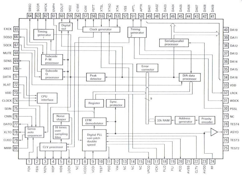
Figure 5.28 Sony CXD2500Q decoder
Sony CXD2500Q decoder
The general operation of the Sony CXD2500Q decoder (Fig. 5.28) is very similar to that of the types previously described, with three main differences: the RAM is now built internally into the decoder; this decoder is capable of variable disc speed operation; and the VCO frequency is derived from the main crystal, instead of a conventional PLL oscillator.
Variable speed or pitch operation
Some manufacturers provide a high speed dubbing of disc to tape facility (Fig. 5.29), whilst some also provide a variable pitch facility which can be used for Karaoke purposes.
Hi-speed dubbing
CD players that have a hi-speed dub facility (Fig. 5.29) are normally part of a 'stack' or 'midi' system, together with a tape deck facility. When this feature is selected, the disc and tape will operate at twice the normal speed. Providing all CD player processing Circuits are linked to the main reference crystal, usually of 16.9334 MHZ, then the crystal timing circuits are altered to provide twice the normal operating frequencies, which will enable the disc to rotate at twice the normal speed, as well as all the relevant digital processing circuits.
The two HCCRS signals from the system controller (one is high, the other is low) will operate the relevant circuits.
It is, however, necessary to alter the gain of both the RF amplifier and CLV stages to provide
Figure 5.28 Sony CXD2500Q decoder
The general operation of the Sony CXD2500Q decoder (Fig. 5.28) is very similar to that of the types previously described, with three main differences: the RAM is now built internally into the decoder ; this decoder is capable of variable disc speed operation; and the VCO frequency is derived from the main crystal, instead of a conventional PLL oscillator .
Variable speed or pitch operation Some manufacturers provide a high speed dubbing of disc to t ape facility (Fig. 5.29), whilst some also provide a variable pit ch facility which can be used for Karaoke purposes.
Hi-speed dubbing
CD players that have a hi-speed dub facility (Fig. 5.29) are normally part of a 'stack' or 'midi' system, together with a tape deck facility. When this feature is selected, the disc and t ape will operate at twice the normal speed. Providing all CD player processing circuit s are linked to the main reference crystal, usually of 16.9334 MHz, then the crystal timing circuit s are altered to provide twice the normal operating frequencies, which will enable the disc to rot at e at twice the normal speed, as well as all die relevant digital processing circuit s.
The two HCCRS signals from the system con t roller (one is high, the other is low) will operate the relevant circuit s.
It is, however , necessary to alter the gain of both the RF amplifier and CLV stages to provide
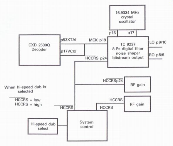
Figure 5.29 High speed dubbing basic block diagram the required operating
characteristics when the disc is functioning at twice the normal speed.
Variable pitch operation
As shown in Fig. 5.30, an output from pin 16 of the decoder, VCPO, is part of a PLL circuit, and is in fact the phase detector signal which is the result of the VCO signal, and is centered on 16.9344 MHz, but variable between 13.26 and 19.78 MHz, being compared with the crystal frequency of 16.9344 MHz. Within the decoder the resultant frequency modifies the crystal timing circuits to provide slightly different frequencies at which the disc speed and data processing circuits function, thereby providing a variation in the pitch of the output signal.
Digital VCO operation
As with previous players employing the earlier decoders, with the CXD2500Q decoder there is no facility for adjusting the VCO. The circuit illustrated in Fig. 5.31 shows an internal VCO which is operating at 34.5744 MHZ (8 X 4.3218 MHz). A crystal oscillator input of 16.9344 MHz is divided by 48 to provide a frequency of 352.8 kHz, and the same frequency is obtained by dividing 34.5744 MHz by 98. The resultant output from the phase comparator at pin 20 is passed via the filter circuit to pin 22 to provide accurate control of the VCO. The main reason for using this method is that the VCO can also be used in the variable pitch function of some of the later players.
Sony CXD2515Q decoder
Figure 5.30 Variable pitch basic block diagram
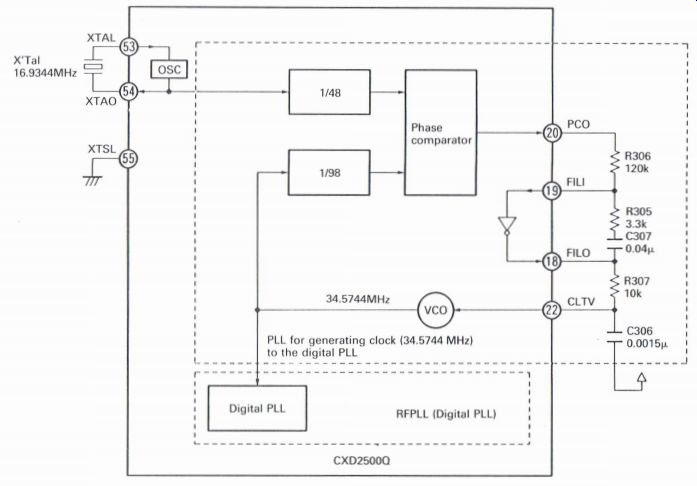
Figure 5.31 Digital VCO operation
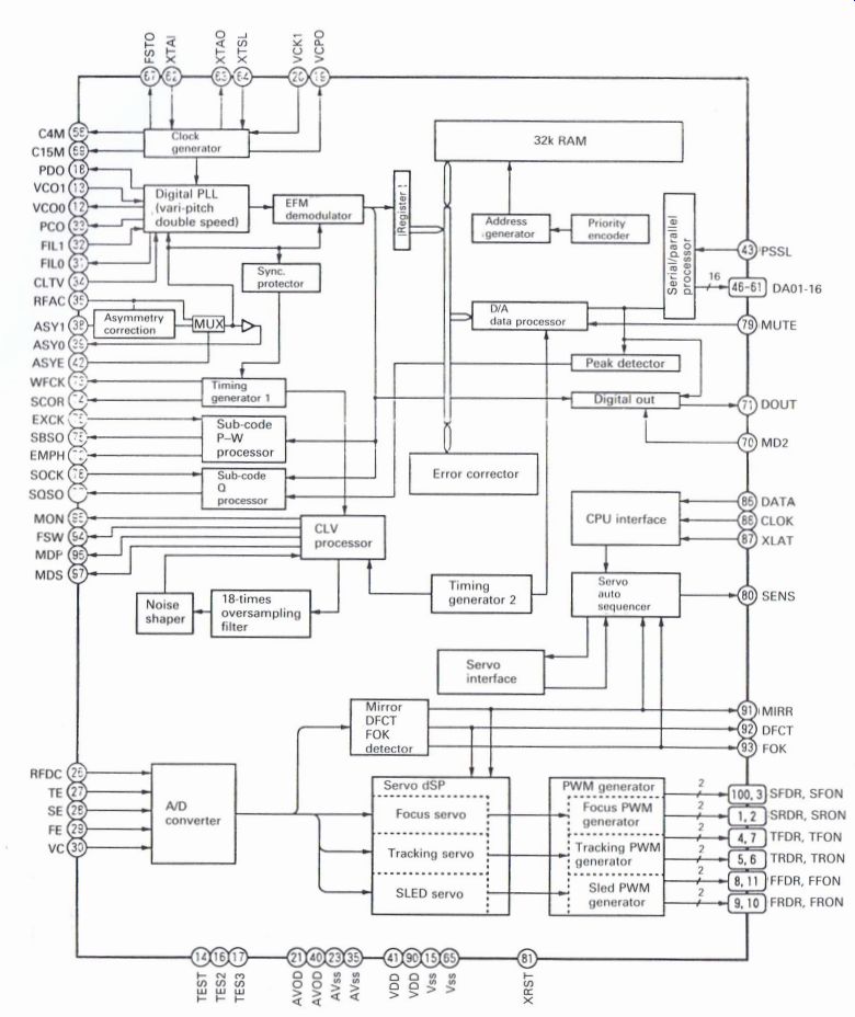
Figure 5.32 Sony CXD2515Q decoder
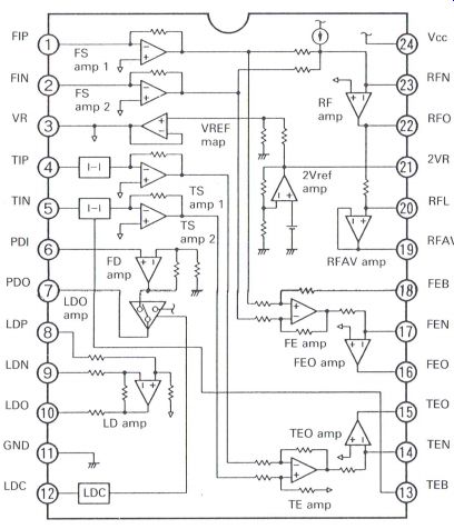
Figure 5.33 RF amplifier TA8137
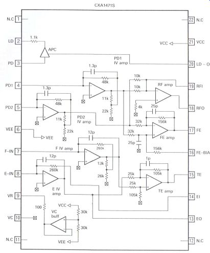
Figure 5.34 RF amplifier CXA1471S
The Sony CXD2515Q decoder (Fig. 5.32) is one of the latest decoder ICs to appear in the more recent CD players, and is an indication of component density, with this IC being a 100 pin quad package. The actual size is virtually the same as that of previous types that appear on the printed circuit board. Included in this package are all the previous functions, plus the digital filter circuits, as well as the servo processing section.
The servo section contains automatic adjustment of all relevant servo correction requirements.
The players that include this IC will have virtually no adjustments, with the possible exception of lateral/radial adjustments as and when a new optical block is fitted.
The various circuit sections that have been described in this section are intended to help engineers gather an appreciation of other types of ICs that perform similar functions, a selection of which have been included in Figs 5.33-5.39.
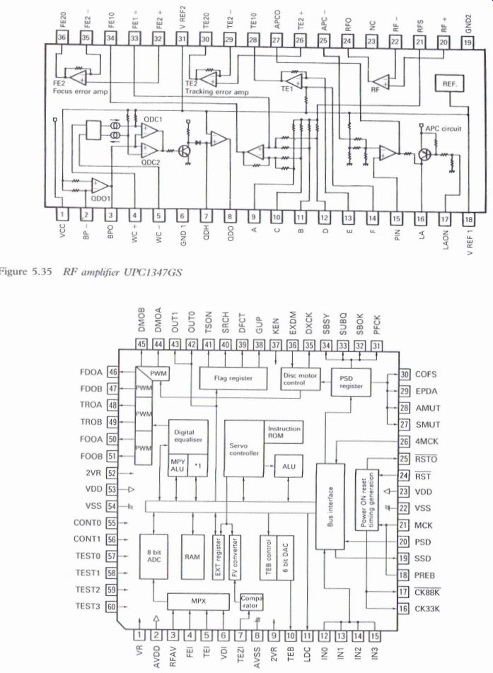
Figure 5.35 RF amplifier UPC 347GS
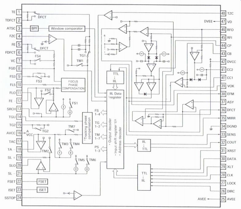
Figure 5.36 Servo amplifier TC9220F

Figure 5.37 Servo amplifier CXA 13728
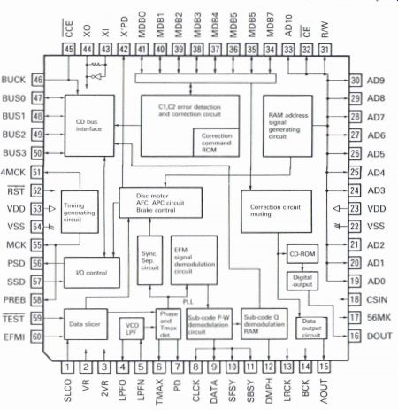
Figure 5.38 Decoder TC922IF
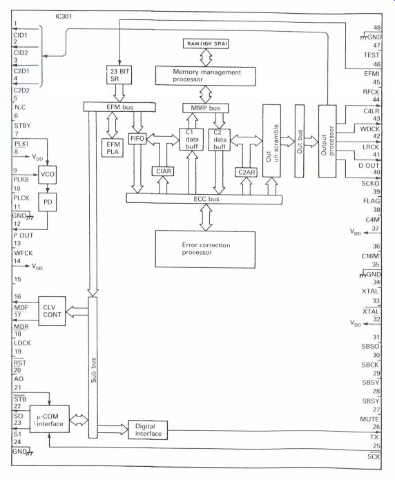
Figure 5.39 Decoder UPD6375CU
------------------