A wide range of publications are available, especially in the reference sections of the larger public libraries, that will cover in depth all the relevant intricacies concerning the principles of processing the analog signal into digital, and back into its hopefully original analog form once again.
Many factors have to be considered when endeavoring to analyze most of the concepts of digital processing, the majority of which is very mathematical. The following information is aimed at providing a basic outline of some of the processes involved, leaving the reader to investigate further depending upon the amount of personal and/or individual desire to proceed further.
Analog to digital conversion -- a few initial thoughts
When an analog signal is converted, or quantized, into a digital form, that analog signal is sampled at certain intervals, and each interval is stored for a brief period of time in a sample and hold circuit, whilst a digital processing circuit converts that level into a specific data word of so many 'bits'. Both circuits are driven by a clock circuit to provide a fixed reference source (Fig. A1.1).
As outlined in Section 1, the original analog data are converted into 16 bit data words, which after further processing techniques are, in effect, implanted onto the disc, and then processed back into analog form within the relevant circuits of the CD player. It would therefore seem logical to consider analog to digital conversion techniques
first, but logic does not necessarily prevail, as it can prove easier to get the 'feel' for this subject by considering digital to analog first; there is also the fact that some types of A to D converters actually employ some D to A processing to enable the final digital data to be achieved.
Digital to analog conversion
The 16 bit data words from the disc, which are developed within the decoder of the CD player from the complex information on the disc, are processed within a general block arrangement as illustrated in Fig. A1.2.
This relatively complex arrangement outlines the processing of the EFM signal from the disc; this is in fact digital information. With processing within the decoder, the original 16 bit data will be extracted from the disc information, but after application via the digital filter, the data words passing to the D to A converter will not usually be in 16 bit form. They will in fact comprise data words in excess of 16 bits due to oversampling techniques as described in the later sections of Section 1.
The fundamentally analog output from the D to A converter is applied to a deglitching circuit to remove undesirable spikes that can develop from the D to A process.
Consider that the input to the D to A converter is a series of data words, with each data word comprising a certain number of bits (which for this example will be 16 bits), and that these bits may be identified as ranging from the least significant bit (LSB), i.e. the lowest value area of the data word, to the most significant bit (MSB), i.e. the largest value area of the data word, as shown in Fig. A1.3.
In order that analog information can be obtained from the digital data it is necessary to consider the significance of each of the data bits when applied to the D to A converter, and this may be considered in the manner shown in Fig. Al.4,
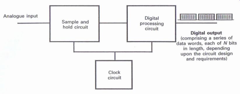
Figure A1.1 Basic principle of analog to digital conversion ----------Digital
output (comprising a series of data words, each of N bits in length, depending
upon the circuit design and requirements)
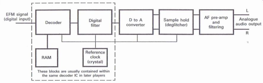
Figure A1.2 Typical D to A processing arrangement of a CD player
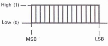
Figure A1.3 Example of a 16 bit data word
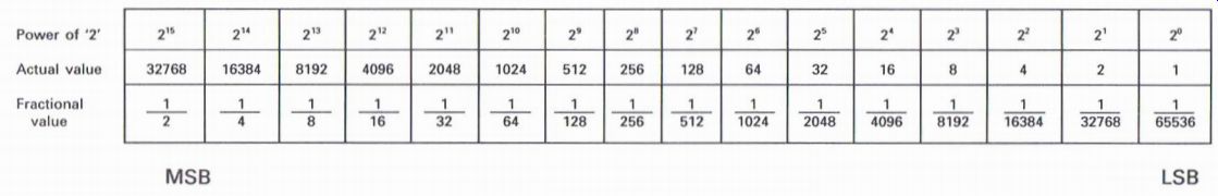
Figure A1.4 Binary number system
Fig. A1.4 provides an overall analysis of the binary system, where each bit of a 16 bit data word is represented as a specific power of '2', with the LSB being the lowest power or value, and the MSB being therefore the highest value.
With a 16 bit data word there are 65 536 possible combinations of the 16 bits from all the 0's through to all the 1's. The LSB will represent the …
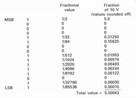
Figure A1.5 Numerical illustration of digital to analog conversion smallest
fraction or value in digital terms, whilst the MSB will represent half
the total possible value. Each of the 1's that may be present in a 16 bit
data word can be analyzed to determine the actual proportion of the original
maximum analog value as follows. Consider the following 16 bit data word,
with the MSB being the first digit, and the maximum analog value for the
purpose of this description being 10 V:
1000110011111011
When the power of 2 increases by one (i.e. 24 to 25), the numerical values these powers represent double (i.e. from 16 to 32), whilst if the power of 2 is reduced by one, the representative numbers will halve. It is these factors which contribute to the operation and accuracy of the digital to analog conversion process.
Basic D to A converter
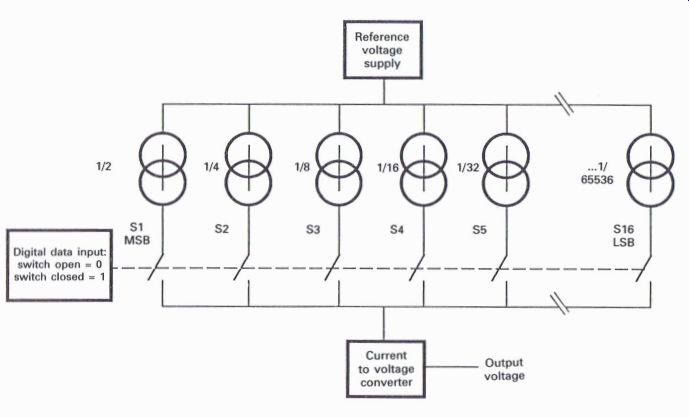
Fig. A1.6 illustrates the basic concept of a D to A converter, which comprises
a series of current generators that are supplied from an accurate reference
voltage source, a series of switches with each one linked to a current
generator, and a current to voltage generator, which will provide an analog
voltage output as a result of the total current that has been created from
the input data word which has closed relevant switches in relation to the
1's information of the data word.
The relation of each current generator is that the most significant bit (MSB) current generator must accurately provide half of the total required current from the reference source, and that the descending generators must again accurately provide half of the current provided by their preceding neighbor. This required accuracy is an essential factor of D to A conversion, and can prove extremely costly when related to domestic CD players, especially when considering the extremely small amounts of current that are required in relation to the least significant bits (LSBs).
Basic resistor ladder D/A converter
With a basic resistor ladder D to A converter (Fig. A1.7) the switches are closed in accordance with the 1's content of the data word to enable a total current to be produced, which will in turn develop an analog voltage output that will ideally replicate the original analog sample.
Unfortunately there are a couple of problems with this method, as well as the following R-2R resistor ladder circuit shown in Fig. A1.8.
1. It is difficult to produce resistors that have an absolute accuracy of each resistor being either exactly double or half the value of its neighbor, with virtually no. variation in tolerance. For example, if R0 was 5K in value, then R1 must be 10K and R2 would equal 20K and so forth, through to R16 which would equal 327.68 M9.
Figure A1.6 Basic D to A conversion
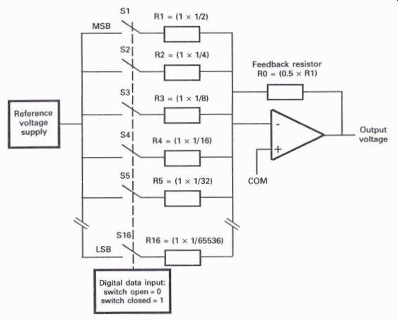
Figure A1.7 Resistor ladder D to A converter
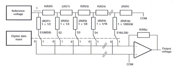
Figure A1.8 R-2R resistor ladder D to A converter
2. When a large number of bits are used in each data word, the range of current inputs from the MSB to the LSB can prove too much for the operational amplifier to handle, especially where the lower order bits are involved. For example, if the reference voltage is 10 V, then the current flow through R1 at 10K will be 1 mA, whilst the current through R16 at 327.68 M-o would equal ~ 0.3 uA.
Basic R-2R resistor ladder D to A converter
The R-2R resistor ladder D to A converter (Fig. A1.8) comprises a set of series resistors, (R20), (R21), (R22), etc., and a set of shunt resistors, (R1), (R2), (R3), etc., and only two resistor values are required, e.g. R = 10K and 2R = 20K. If the current flowing through the chain of resistors R20 through to Rt is I, then through R1, I = I x 1/2, and through R2, I = I x 1/4 and so forth.
With the switches in the '0' position the lower end of the resistors R1 through to R16 are connected to common or ground, and when set to the '1' position the 'virtual earth' input of the operational amplifier will still maintain the same effect, but of course will comprise the total current which will relate to the 1's information of the data word input.
This method of D to A conversion is in fact easier to manufacture, as only two specific values of resistor are required, i.e. R and 2R.
Typical D to A converter
Fig. A1.9 illustrates the basic D to A converter arrangement used in many players, and is based on a circuit which utilizes the Sony D to A converter IC. This form of D to A converter is often referred to as an integrating dual slope D to A converter. It comprises two constant current generators, one providing I_0 which is related to the eight most (or higher) significant bits, and the other providing I_0 which is related to the eight least (or lower) significant bits.
The current switches are similar to those described in previous basic D to A Circuits, with the resultant current being passed via the integrating circuit, to the relevant left or right sample and hold circuit. Generally the four main inputs to this circuit will comprise: DATA, bit clock, word clock (WDCK) and left/right clock (LRCK).
The DATA will be the 16 bit data word, which will operate the relevant current switches to provide a total current that relates to the analog value of each data word. The bit clock is a constant clock frequency at the relevant data rate to enable the data to be processed correctly. The word clock (WDCK) enables the higher and lower order 8 bit sections of each data word to be processed as required, whilst the left/right clock (LRCK) ensures that the left and right data words are routed through to their respective circuits to provide the final left and right analog outputs (Fig. A1.10).
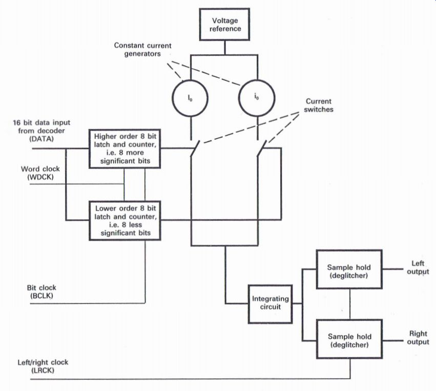
Figure A1.9 Typical D to A converter
Sample and hold circuits
Whilst both the D to A and the A to D conversion circuits operate in a digital manner, it is essential that some form of sample and hold circuits are utilized to help these circuits operate efficiently.
In the D to A process the sample and hold circuit is used to remove undesirable interference, frequently referred to as 'glitches', which can occur at the output of the D to A circuit after the integration of each data word.
With respect to the A to D process, the sample and hold circuit provides a 'sample' of the input analog signal, and then 'holds' it whilst that value is converted into a digital data word.
Basically the sample and hold circuit may be represented as shown in Fig. A1.11, and comprises a couple of switches and a capacitor, with S] switching the analog sample to the capacitor, whilst 82 will discharge the capacitor when the digital conversion has been completed, and before the next sample is selected.
Sampling an analog signal for A to D conversion The analog signal is sampled at regular intervals, and each sample is stored in the capacitor C, whenever S] is closed, whilst 82 discharges the capacitor in readiness for the next sample (Fig. A1.12).
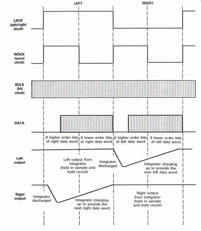
Figure A1.10 D to A conversion timing chart
Whilst each sample is held in the capacitor C, the specific value of each sample will be turned into a digital data word. In practice the switching pulses for both switches will be high in frequency terms, whilst the change of each pulse into a data word of so many bits will be even higher, with the final data frequency being related to the number of bits being used for the data words.
The switches B1 and B2 are usually CMOS type semi-conductor switches which are practical for high frequency operation.
Sampling an analog signal after D to A conversion
When the digital data word is transformed or quantized back into its ideally analog value, it is possible to develop interference pulses as the D
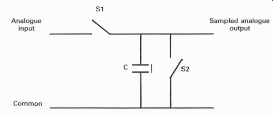
Figure A1.11 Sample and hold circuit
Figure A1.12 Basic sampling of the analog signal
Analog signal to be sampled switching pulses High frequency ' which operate S1
.l Result samples held in the capacitor C. S2 will operate between each sampled pulse to discharge the capacitor in readiness for the next sample
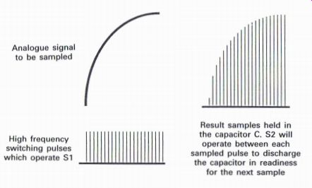
Figure A1.12 Basic sampling of the analog signal to A converter settles
or stabilizes from one data word to the next. This interference can frequently
be referred to as erroneous data, quantizing noise, or even glitches, and
can cause unnecessary noise and possibly distortion of the required analog
signal output. The effect of this can be minimized by using a sample and
hold circuit which is frequently referred to as a 'de-glitcher' (Fig. A1
.13).
Analog to digital conversion
Having considered the basic concepts of D to A conversion, and also some of the principles of sample and hold techniques, it is now convenient to consider some of the basic concepts of A to D conversion.
Basically the requirement is to sample an analog value at regular intervals, and turn those samples into data words, each of which comprises a certain number of bits. The actual number of bits is related to the accuracy that is required of a particular system or method of A to D conversion, and also the frequency range that the system may be required to cover; in the case of CD technology, the required audio range is in the region of 0-20 kHz, with 16 bits in each data word, with each sample of the analog signal being carried out at a sampling frequency of 44.1 kHz. In order that an appreciation can be achieved of how an analog signal is turned into a digital form, consider the following method of A to D conversion.
Successive approximation analog to digital converter
Assume the reference voltage = 10 V, and the analog input = 6.6 V (Figs A1.14 and A1.15).
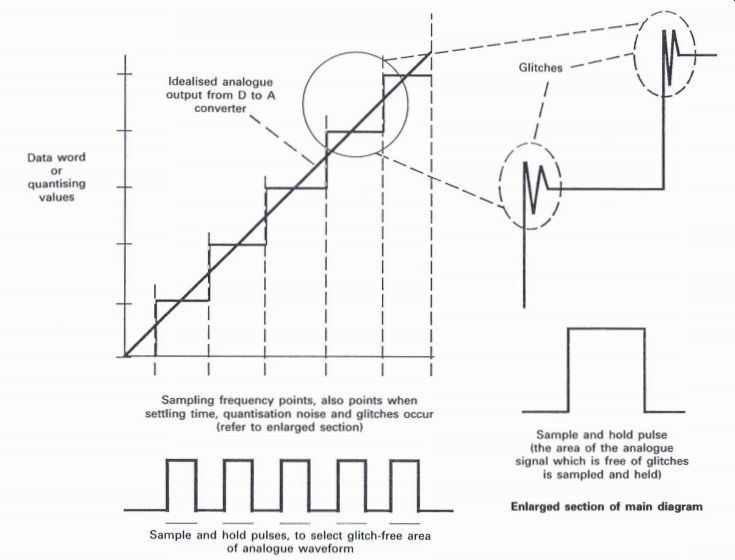
Figure A1.13 Using sample and hold to remove glitches from the analog
output from the D to A converter
Basically the control logic section causes each clock pulse to operate the shift register which applies a series of data bus lines to the D to A converter via the output latches. The data bus lines will provide the relevant digital data word on completion of the analysis of the sampled analog input.
The D to A converter provides successively reducing levels of the input reference voltage of 10 V, which is applied to the converter stage, the output of which will change either high or low depending upon whether the D to A output is greater than, or less than, the input analog input of 6.6 V.
The sequence of operations is as follows:
Stage 1. The start signal is sent, and the first clock pulse sets the data output B1-B8 to 10 000 000, which is equal to 5 V from the D to A converter, to the input (V in) of the comparator. The comparator output remains high as the analog input of 6.6 V is greater than 5 V.
B1 is latched to '1' and held.
~ Stage 2.
The second clock pulse is sent and B2 is set to '1'. Data output B1-B8 is now 11 000 000 = 7.5 V. V in is now greater than 6.6 V, and therefore the comparator output is now low. B2 is now latched to '0' and held.
Stage 3. The third clock pulse sets B3 to '1'.
B1- B8 is now 10100 000 = 6.25 V. V in is now less than 6.6 V, and therefore the comparator output is high. B3 remains latched to '1' and held.
Stage 4. The fourth clock pulse sets B4 to '1'. B1-B8 is now 10110000 = 6.825 V. V in is now greater than 6.6 V, and therefore the comparator output is low. B4 is now latched to '0' and held.
Stage 5. The fifth clock pulse sets B5 to '1'.
Ble8 is now 1010] 000 = 6.562 V. V in is now less than 6.6 V, and therefore the comparator out~ put is high. B5 remains latched to '1' and is held.
Stage 6. The sixth clock pulse sets B6 to 'l'.
B1-B8 is now 10101 100 = 6.718 V. in
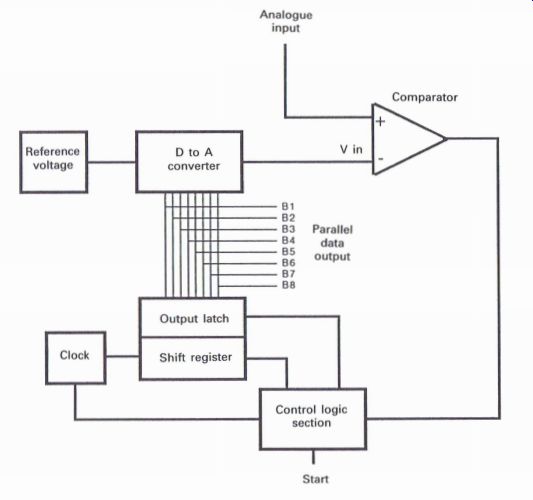
Figure A1.14 Successive approximation A to D converter
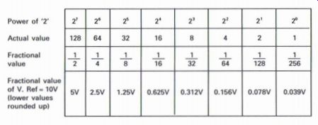
Figure A1.15 8 bit binary table greater than 6.6 V, and therefore the
comparator output is low. B6 is now latched to '0' and is held.
Stage 7. The seventh clock pulse sets B7 to '1'. B1~B8 is now 10101010 = 6.64 V. V in is now greater than 6.6 V, and therefore the comparator output is high. B7 is now latched to '0' and held.
Stage 8. The eighth clock pulse sets B8 to '1'.
B1-B8 is now 10101001=6.601 V. V in is now greater than 6.6 V, and therefore the comparator is high. BS is now latched to '0' and held.
Stage 9. The next clock pulse completes the operation and the final data word of 10 101 000 is the data word output. The system awaits the next start signal to commence the operation on the next analog input. Engineers studying this section are invited to calculate data outputs for alternative analog inputs, especially for inputs that are less than half the reference voltage potential.
Binary counter A to D converter
Compared to the previous description, the binary counter A to D converter (Fig. A1.16), though fundamentally similar in design, is much simpler in operation.
Again a reference voltage is applied to the D to A converter, but the control logic causes the clock to commence operating a binary counter which commences counting from zero (i.e. B1-B8 = 00 000 000) upwards until an output from the D to A converter produces a voltage input (V in) to the comparator which is greater than the analog input, at which time the comparator will ...
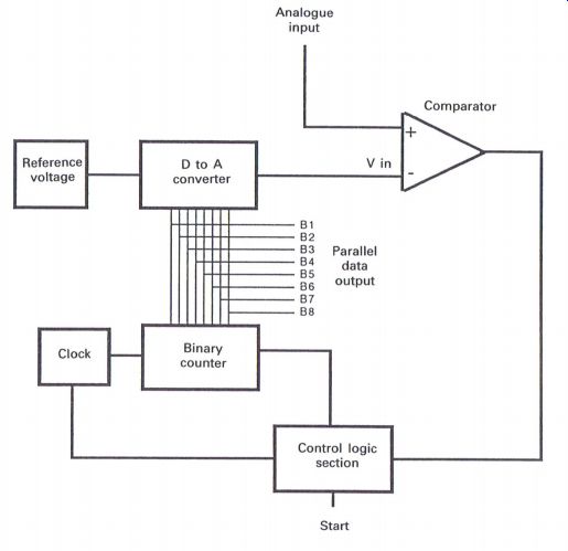
Figure A1.16 Binary counter A to D converter change the output level from
high to low, which in turn causes the binary counter to stop the counting
sequence, and the data output, B1-B8, at that point must approximate to
the value of the analog input.
Dual slope A to D converter
The circuit shown in Fig. A1.17 essentially comprises an integrator which will enable the capacitor C to charge up to the analog value from the sample and hold circuit, a comparator which controls a clock driving a binary counter, and a logic control stage to ensure the complete circuit operates in the correct logical sequence.
Before a start signal is applied, S2 will be closed to ensure that the capacitor C is discharged. When the start signal is applied, S2 will open, whilst S1 will switch over to enable the analog input from the sample and hold circuit to charge up the capacitor towards the analog level, during the time (t0-t1). As the charging commences (Fig. A1 . 18), the clock pulses will drive the binary counter for a set period of time which is also (t0-t1).
At time t1, B1 will change over to the reference voltage input, the binary counter will be set to zero, and as the capacitor C changes its charge towards the reference voltage, the binary counter will now commence counting, until the point at which C is discharged, at time (t2), when the comparator output will change over, stopping the clock operation.
The binary counter is held at that moment and will be an indication of the digital value of the analog signal input.
Accuracy of analog and digital processing circuits
Whether a designer is considering analog to digital conversion or vice versa, the accuracy of the conversion circuits is extremely important.
Whilst the equipment for A to D conversion in ...
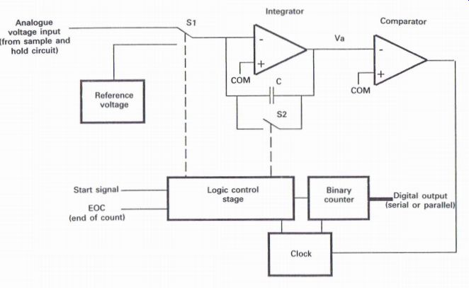
Figure A1.17 Dual slope A to D converter
S1 switched to reference voltage, binary counter now counting from zero, and will stop at 1'2, when C is discharged.
... to S1 switched to analog input, and C charging up.
Binary counter running for a specified time
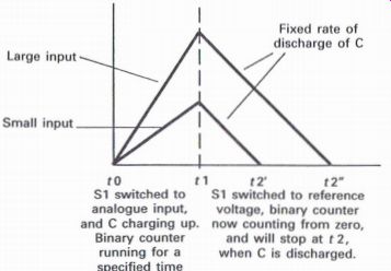
Figure A1.18 Timing sequence
of the dual slope A to D converter the recording studios may achieve
an excellent quality of accuracy due mainly to a high standard of equipment
which will no doubt result in accurate conversion of the analog signal
into its digital counterpart, it is in the CD player that absolute accuracy
may not be achieved in view of the fact that the retail price of a player
will most certainly not reflect the true cost of the technology needed
to achieve the accuracy that may be required.
Because D to A converters for CD players are difficult to design whilst maintaining cost restraints, the latest trends towards the use of one bit, pulse-flow, and bit stream techniques have resulted in a very effective method of D to A conversion which generally maintains a high degree of accuracy at a much reduced cost involvement, despite the technology involved, generally due to modern mass production methods.
Analog to digital accuracy problems
The ideal response of the A to D converter is shown in Fig. Al.19, which illustrates the ideal condition of specific voltage levels, enabling a different data word to be provided, i.e. 5 V = 100 and 8.75 V = 110, etc. If a different level of voltage were to provide an incorrect data word, due to non-linearity, then the incorrect analog value would be obtained during the D to A conversion process.
This problem can be reduced by using an increased number of steps between the minimum and maximum analog levels, which in turn would require data words of more bits.
In CD technology where 16 bit data words are used, there are 65 536 variations of the 16 bit
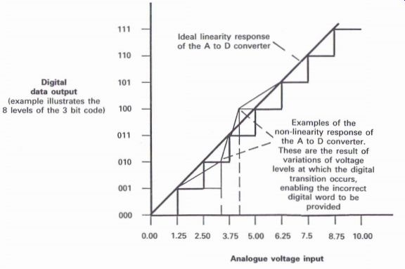
Figure A1.19 Linearity requirements of the A to D converter
---------Digital data output (example illustrates the 8 levels of the 3 bit code)
Examples of the on-linearity response of the A to D converter.
These are the result of variations of voltage levels at which the digital transition occurs, enabling the incorrect digital word to be provided
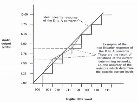
Figure A1.20 Linearity requirements of the D to A converter ---
Examples of the non-linearity response of the D to A converter.
These are the result of variations of the current determining networks, i.e. the accuracy of the resistors which determine the specific current levels
Analog voltages
These levels are related to the values of the resistors R in the chain.
Each resistor can be considered to be related to a specific data word in the D to A conversion stage. Therefore if any resistor is not accurate in providing a specific potential, then in this basic illustration all other potentials can be affected, and can indicate problems that can occur in the accuracy requirements of the D to A converter
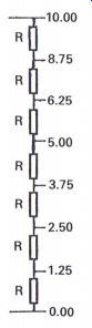
Figure A1.21 Fundamental illustration of the accuracy requirements of
the D to A converter codes from all the 0's through to all the 1's, which
implies there are the same number of intermediate steps from the minimum
to maximum values of the analog signal which is probably much smaller in
value than the 10 V range illustrated in Fig. A1.19.
Digital to analog accuracy problems
The ideal response of the D to A converter is shown in Fig. A1.20, which illustrates the ideal condition of providing specific voltage levels which are the result of a range of current determining circuits, e.g. resistors, with each specific current being related to a particular data word. As illustrated in Fig. A1.21, if one or more of the resistors in the chain is not absolutely accurate in order to produce a defined voltage, then the voltages throughout the chain will not be at the required level.
In similarity to the A to D accuracy problem this problem can be reduced by using an increased number of steps between the minimum and maximum analog levels, which in turn requires data words of more bits. But unfortunately the cost of producing such accurate resistors can prove to be extremely high, especially for the domestic product range of CD players.
------------------